CoSi chip interconnects — one-tenth copper resistivity at 20 nm, but cheaper chips?
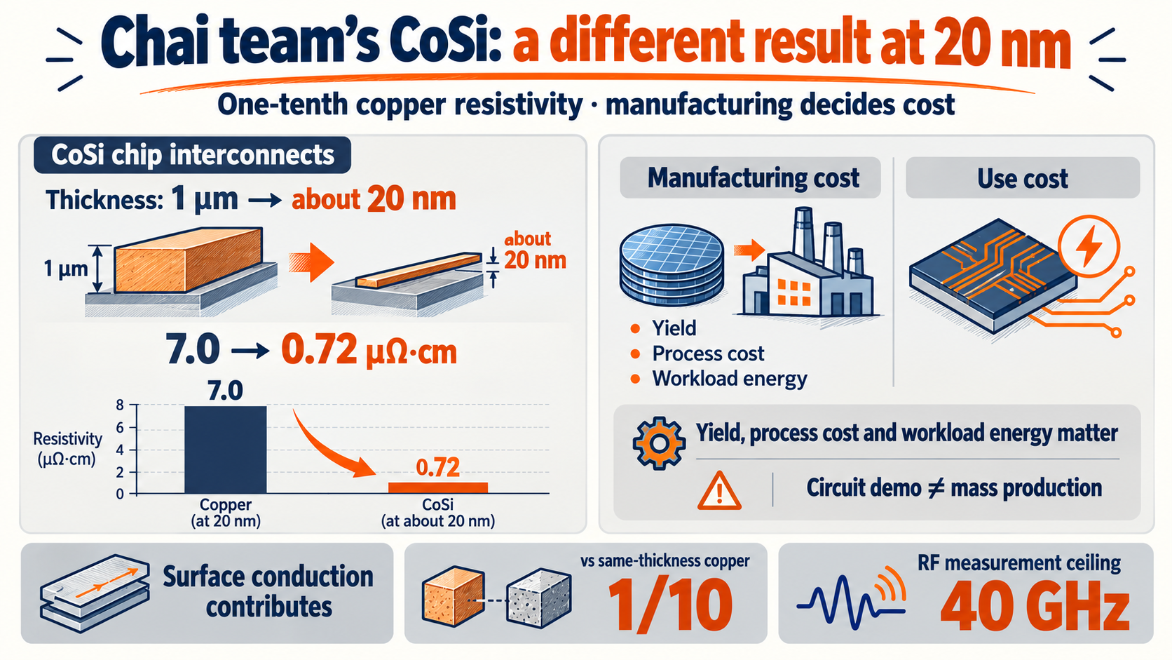
Yang Chai and colleagues at The Hong Kong Polytechnic University have reported a promising result for CoSi chip interconnects: at about 20 nm thick, the material had one-tenth the resistivity of copper at the same thickness. The economic question is how much of that material advantage can survive fabrication and reach a working chip. Source: Nature Materials
Interconnects carry electrical signals between transistors. Faster switches are less useful if their connections delay the signal. Shrinking a chip therefore requires better wiring as well as smaller transistors. Source: Applied Materials · 2026
The paper appeared in Nature Materials on September 8, 2026, followed by a commentary on September 25. Its appeal is a way to improve electrical behavior as a material gets thinner. That is an early research advantage, with manufacturing still to be established. Source: Nature Materials · News & Views
The people behind the work
Chai supervised the project as corresponding author. Joint first authors Jiewei Chen and Jianmin Yan contributed to resistivity experiments and analysis; Chen also worked on the concept, calculations and high-frequency measurements. These roles are specified in the paper’s contribution statement. Source: Nature Materials
The lab has a history of turning low-dimensional materials into devices. Its publication list includes work with Chen on tellurium phase-change transistors in Science Advances in 2022 and motion-perception devices in Nature Nanotechnology in 2023. That background helps explain the move from material measurements toward circuit integration. Source: Yang Chai 연구실
How CoSi chip interconnects differ from copper
In very thin copper, electrons scatter more at surfaces and crystal boundaries, making current harder to carry. Resistivity describes the material’s opposition to current. A wire’s actual resistance also depends on its length and cross-sectional area. Source: 논문 보충자료 · Note 1
The CoSi studied by Chen and Yan is a cobalt–silicon semimetal, with an electronic structure different from a conventional metal. The authors attribute its behavior to a highly conductive surface path whose relative contribution grows as the material becomes thinner. Source: 논문 보충자료 · Notes 1, 3
Reported CoSi resistivity falls from 7.0 μΩ·cm at 1 μm thickness to 0.72 μΩ·cm at about 20 nm. The chart compares CoSi samples of different thicknesses. The copper comparison in the headline is a separate, same-thickness benchmark reported by the authors. Source: Nature Materials
Reported CoSi values at different thicknesses, not wire resistance or chip power savings.
Lower resistivity helps, but a thinner wire also has less cross-sectional area. The complete connection must still be measured with its actual length, width and contacts. A favorable material trend does not remove the effects of geometry.
A circuit demonstration, with a narrower claim
High-frequency measurements involving Chen and Kevin J. Chen reached 40 GHz. A separate demonstration connected CoSi to a silicon ring oscillator made at the 16 nm technology node. This test circuit repeatedly circulates a signal; it ran at the same frequency as its metal-connected counterpart. Source: Nature Materials
The dimensions describe different things. The 20 nm value is material thickness; the 16 nm node names the silicon process generation. Supplementary Note 5 gives the CoSi RF test device a width of 4.5 μm. Its 40 GHz result is neither a 20 nm-wide wiring demonstration nor a CPU clock speed. Source: 논문 보충자료 · Notes 5, 6
Paper and supplement
Low resistivity at 20 nm thickness
Material
RF · Measurements up to 40 GHz
Circuit · Same frequency as metal-connected circuit
Further validation
Replication in narrow lines and contacts
Patterning
Power · Energy per real workload
Manufacturing · Production yield and total process cost
The same distinction matters for economics. Lower resistive loss can help power delivery and signaling, but computing, memory access and other connections also consume energy. A material’s resistivity ratio cannot be used as a server electricity-bill reduction.
The next challenge for Chai’s team is manufacturing
Moving Chai’s result into a factory requires reproducible material growth and integration. The supplement gives an optimal growth window of 860–890°C for thin flakes. Applying the material to completed transistor and dielectric structures requires a separately validated process that preserves them. Source: 논문 보충자료 · Note 2
Growing it elsewhere and transferring it is one possible route to investigate—an industrial inference, not a manufacturing result established here. Transfer damage, contamination and alignment could add costs. Better material performance and cheaper fabrication are separate achievements.
Patterning a broad thin flake into a narrow wire presents another challenge. The supplement discusses surface defects and lateral confinement as possible reasons for poorer nanowire behavior. Performance after patterning and encapsulation is therefore a key manufacturing question. Source: 논문 보충자료 · Note 3
Copper and ruthenium are moving targets
Chai’s work enters an industry that is already improving its alternatives. In 2024, Applied Materials reported up to 25% lower line resistance using a ruthenium–cobalt liner for copper. The approach improves the space available to copper and how it fills the structure. The performance figure is a company claim. Source: Applied Materials · 2024-07-08
In its January 2026 technology discussion, Applied Materials also emphasized copper’s manufacturing maturity and compatibility. A prospective CoSi customer would compare it with further improvements to a familiar process. The baseline keeps advancing. Source: Applied Materials · 2026-01-23
Imec has published manufacturing metrics for ruthenium. In June 2025 it reported that 40% of its 16 nm-pitch structures met a resistance target, while 18–22 nm-pitch structures achieved full-wafer yields of at least 90%. Pitch is the repeating spacing between neighboring lines, not the CoSi thickness or silicon node. Source: imec · 2025-06-03
16 nm-pitch Ru
40% of structures met resistance target
Metric
Meaning · Uniformity challenge at tighter pitch
18–22 nm-pitch Ru
Full-wafer yields ≥90%
Metric
Meaning · Results at wider spacing
These are different experiments, so they do not rank CoSi against ruthenium. They show what a manufacturing evaluation eventually demands: low resistance across many structures, delivered consistently.
Manufacturing cost and computing cost may move differently
Assuming Chai’s result can be industrialized, start with the manufacturer’s accounts. Cost per good die can be viewed as total wafer processing cost divided by the number of saleable chips. Added process expense or lower yield can raise that cost even when electrical performance improves.
If wiring improvements allow designers to reduce margins, they could potentially fit more functionality into the same area. They might also reduce failures caused by inadequate connections. Both possibilities need design and production evidence; neither is a measured cost saving in this paper.
A data-center buyer has a different calculation. A more expensive chip could still cost less over its lifetime if it completes the same work with less energy or in less time. That requires workload-level energy and throughput measurements, beyond a favorable result in one connection.
-
1
After fabrication
Retain benefits in narrow wires and contacts
-
2
Cost per good die
Account for added steps and yield
-
3
Real workloads
Measure energy and execution time
-
4
Lifetime cost
Combine purchase and operating costs
Potential new business could extend from material supply to uniform-film equipment, fine-line etching and surface or defect inspection. Those are plausible areas for Korean equipment and materials firms to investigate. The reviewed sources do not establish a CoSi order or adoption plan for any particular Korean company.
Wholesale replacement of the copper industry is an unlikely inference from this study. Different connections within a chip have different requirements. A more plausible industrial scenario is selective use in the smallest, most demanding locations while familiar metals remain elsewhere. It does not imply a collapse in commodity copper demand.
What to watch next: reproducibility in narrower wires
Chen and Yan’s experiments give a reason to investigate thin CoSi as a wiring candidate. Useful follow-up evidence would include actual line dimensions, wafer-wide distributions and resistance including contacts. Lifetime data with stated test durations and comparative processing costs would make the economic case more assessable.
For better wiring to produce cheaper computing, its advantage must survive both fabrication and use. This CoSi chip interconnect study offers a concrete starting point. The savings still have to be earned through the next experiments and process development.
Sources were checked as of September 30, 2026. The abstract was checked through PubMed and the supplement through the publisher. The contribution statement was consulted through an indexed reproduction of the public article page, with authorship cross-checked against the university lab list; the subscription-only main text was not fully accessed. Industry figures are identified as company or institute reports. Cost and market implications are conditional editorial analysis.
Better wiring reduces computing cost only if its advantages survive manufacturing.
Sources and further reading
For information only — this is not a recommendation to buy or sell any asset.
Comments 0