Perovskite solar cells hit 26.5% by melting grain boundaries — when will factory costs move?
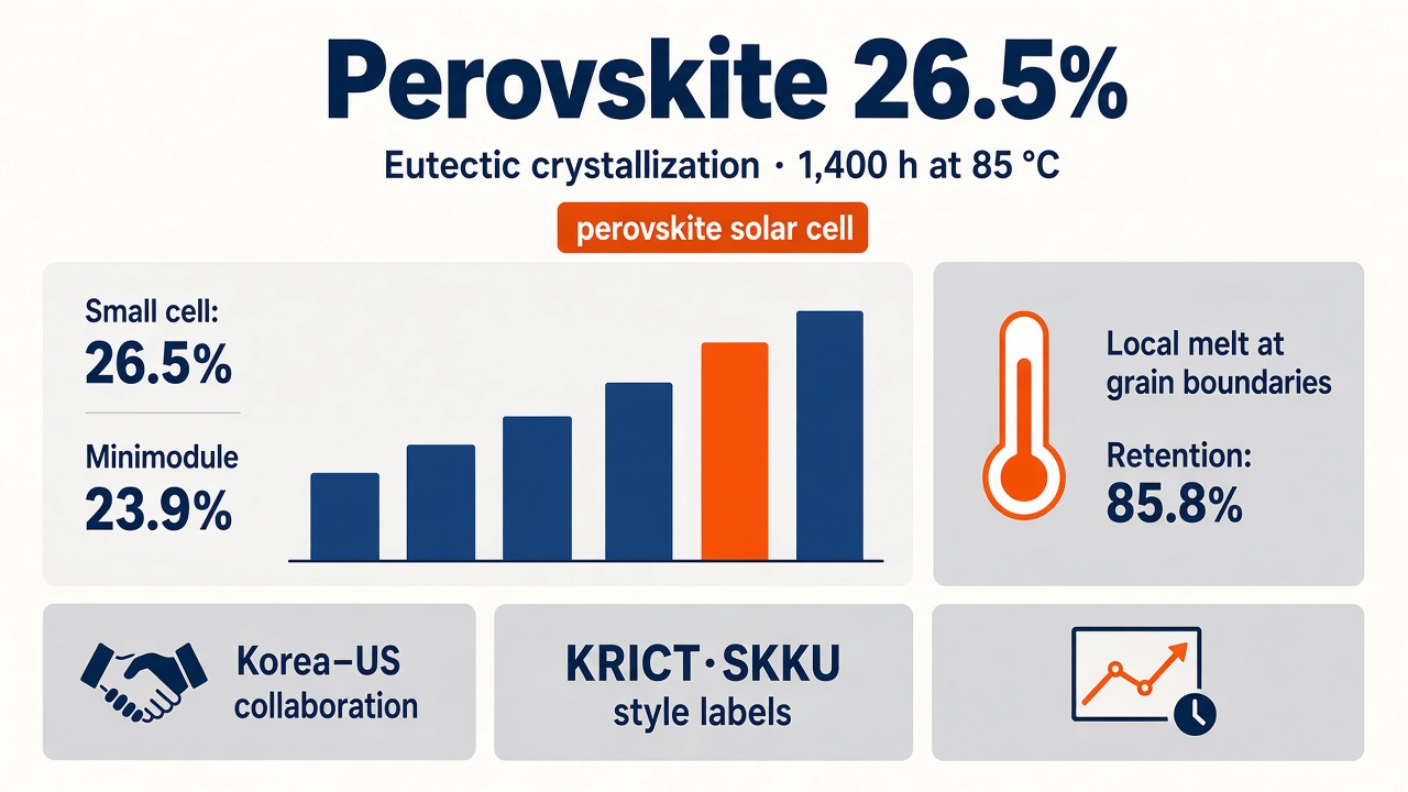
On October 8, 2026, Jason J. Yoo at the Korea Research Institute of Chemical Technology (KRICT) and corresponding author Seong Sik Shin at Sungkyunkwan University, with a large Korea–US team, published a volatile-eutectic route to control perovskite solar cell crystallization in Science. Small-area solar cells reached 26.5% power conversion efficiency (25.9% certified), minimodules above 15 cm² reached 23.9%, and cells kept 85.8% of their initial efficiency after 1,400 hours of continuous operation at 85 °C. This article separates what the paper proves from what factory cost and bankability still require. Source: Science · 2026-10-08
This is not a recommendation to buy any stock or module. Treat lab data and industry roadmaps as different layers.
Who led the work — Yoo, Dolan, Shin, and Noh
Co-first authors are Yoo at KRICT, Connor J. Dolan at UC San Diego, and Seongsik Nam on Shin’s team at Sungkyunkwan University. Yoo, Dolan, Shin, David P. Fenning (UCSD), and Dane W. deQuilettes (MIT/Princeton) conceived and designed the experiments; Shin, Fenning, and deQuilettes are corresponding authors. Fenning’s side designed the synchrotron nanoprobe and eutectic-melting experiments, while Nam handled film structure and morphology, minimodule fabrication, and electroluminescence. Jun Hong Noh at Korea University extracted optical material parameters from the films. Source: Science · Authors
Yoo and Shin already reported high-efficiency perovskite cells via carrier management in Nature in 2021. Here they move upstream into how salts in the ink reshape crystals during annealing (the bake that sets the film). Noh is a long-standing name in Korean halide perovskite efficiency work and this time supplied the optical constants used to interpret efficiency and voltage loss.
Why perovskites stall — recombination at grain boundaries
Perovskite photovoltaics use a thin crystal film to absorb light and separate charge. Grain boundaries are where carriers trap or disappear, hurting voltage and efficiency. The abstract reports higher photoluminescence quantum yield, longer carrier lifetimes, and lower surface recombination velocity — the same fight in different metrics.
Earlier routes used surface passivation (coating defects so charges do not leak away) liquids or volatile methylammonium chloride to grow grains. This team uses a eutectic between zinc bromide and MACl to locally melt grain boundaries during annealing, ripen grains, and then leave a cleaner film as volatiles escape.
-
1
Ink additives
ZnBr2 + MACl form a eutectic interaction
-
2
Annealing
Local melt at grain boundaries lowers defect density
-
3
Zn segregation
Zn moves to boundaries/interfaces; passivates nonradiative defects
-
4
Volatility
Additives leave, leaving a cleaner crystal film
What is different about a volatile eutectic
Science’s editor summary states that local melting of the eutectic at boundaries during annealing enhances grain ripening and cuts intragranular defect density, while zinc segregates to boundaries and likely passivates nonradiative defects. Fewer residues after volatilization matter for manufacturing: extra rinse or bake steps are real dollars on a line. Source: Science · Editor’s summary
The Fenning–Dolan nanoprobe X-ray work maps element distribution at grain boundaries versus grain interiors. That is not the same as blindly raising anneal temperature on the whole panel. It ties into the long-standing goal of approaching the Shockley–Queisser limit (the ~33% theoretical ceiling for a single-junction cell) by cutting charges that vanish without emitting light.
Shin and Nam’s numbers — 26.5% cells, 23.9% minimodules, 1,400 h at 85 °C
26.5% is the lab’s own measurement; 25.9% is the value re-measured by an outside certifier — the usual two-layer truth for record cells. 23.9% on minimodules above 15 cm² answers part of the ‘only tiny pixels work’ critique, though areas are still far below standard silicon modules.
Bars are % PCE or retention. 85.8% is retention vs initial 24.1% PCE.
Stability is conditional: PTAA hole-transport cells at 24.1% initial PCE retained 85.8% of that value after 1,400 h at 85 °C continuous operation. That is not a 25-year outdoor warranty. Still, 85 °C is roughly what a module on a summer rooftop sees, and it stresses the encapsulant (the layer sealing out moisture and oxygen).
The same chemistry delivered 26.1% external quantum efficiency in LEDs — a hint that deposition and anneal tools could serve both solar and display pilots in Korea.
Commercialization is another layer — Qcells and GCL
In 2026, perovskite–silicon tandems are judged both on lab efficiency and on whether banks finance modules. In July Qcells said it was the first to earn TÜV Rheinland IEC/UL 61215 (durability under heat, humidity, load) and 61730 (electrical safety) certification for perovskite tandem tech — a standards story, not a specific ink recipe. Source: PV Tech · Qcells
GCL Optoelectronics reportedly won a 1.2 MW Huaneng commercial tandem tender in March with requirements above 25% efficiency, IEC certification, and a 25-year performance warranty. That tender is not this paper’s product, but it shows price is set by certification, warranty, and gigawatt lines — not a single efficiency press release. Source: pv magazine · GCL
This Science paper
26.5% PCE
Small cell
Heat stress · 85 °C, 1,400 h continuous
Area · >15 cm² module 23.9%
Commercial module talk (external)
IEC 61215/61730 etc.
Certification
Warranty · 25-year performance (tender terms)
Cost · Not in paper
When Korean factory costs move — deposition, anneal, yield
Having KRICT, SKKU, and Korea University on the author list is relevant for Korean pilot lines, where anneal windows and uniformity dominate scrap. If a eutectic additive widens the process window or cuts defects, good die area per pass rises and rework falls. Cost per watt ($/W) is not in the paper; it moves only when yield, encapsulation, and lifetime multiply together.
Our earlier piece on Related: screen-printed perovskite at 21.86% stressed process over headline efficiency. This Science result is another lever on ink and anneal. The Related: autonomous lab and 27.22% cell story cuts experiment iteration cost; this one raises film quality per anneal. Both must align before R&D and pilot spending change.
Related: Solar desalination showed a different use of photovoltaic output. Higher cell efficiency helps only if heat, membranes, and O&M still close the water cost — do not paste these cell numbers into that model blindly.
What the paper proves — and what it does not yet
- Verified: ZnBr2+MACl eutectic crystallization; 26.5% small cell (25.9% certified); >15 cm² minimodule 23.9%; 85.8% retention after 1,400 h at 85 °C (Science abstract).
- Verified: 26.1% LED EQE on the same platform.
- Verified: corresponding author deQuilettes co-founded perovskite metrology startup Optigon; a related US patent application (64/117,376) is listed in the paper’s competing interests.
- Conditional outlook: better anneal yield could cut scrap on Korean pilot lines if additive, cleaning, and encapsulation costs do not dominate.
- External outlook: Qcells/GCL certification and tenders open commercial tandems; no report that this ink ships in those products yet.
Module and investment choices depend on your site and risk tolerance. The next evidence this material needs for factory P&L is large-area derating, IEC stress suites, and encapsulation lifetime — not another half-point on a coupon cell alone.
26.5% is a starting point; $/W moves only when yield, encapsulation, and certification align.
Sources and further reading
For information only — this is not a recommendation to buy or sell any asset.
Comments 0