7eV oxide semiconductor: can an insulating material change power-device costs?
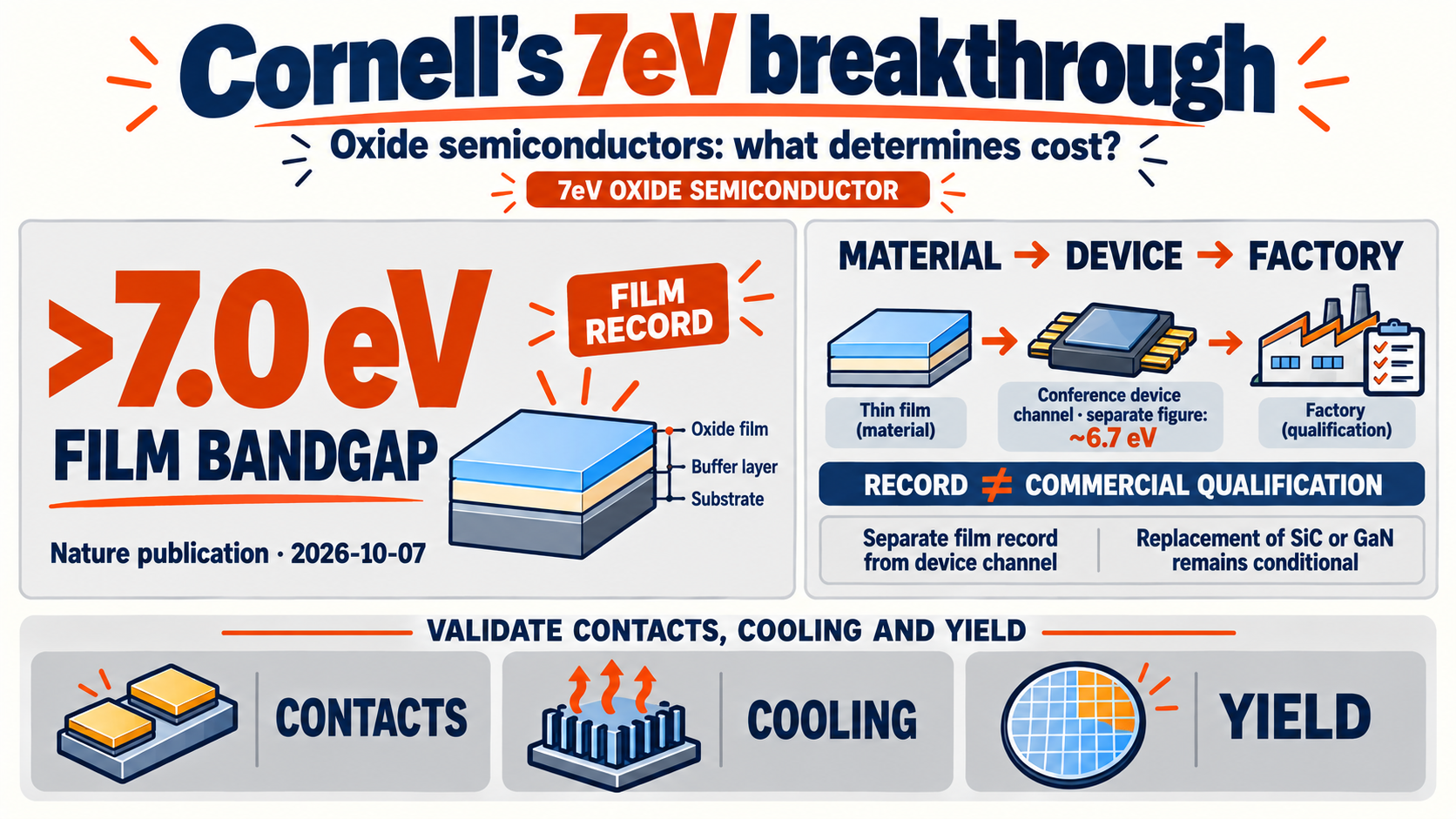
A 7eV oxide semiconductor reported in Nature on October 7 by Cornell’s Darrell G. Schlom, Jacob Steele and Debaditya Bhattacharya expands the range of materials in which electrical conduction can be controlled. It adds a candidate for future power electronics. Turning that materials result into lower electricity bills or manufacturing costs will require further device and factory validation. Source: Nature · 2026-10-07
An EV charger or factory motor cannot simply use electricity exactly as it arrives. Conversion equipment changes its voltage or waveform. Power semiconductors switch current or guide it in one direction. They must conduct with little loss when on and withstand voltage when off. A useful device has to do both well.
Who did what in Schlom’s lab
The project joins materials growth to device engineering. Equal-contribution authors Steele and Bhattacharya led film growth and electrical measurements, and device fabrication and testing, respectively. Kazuki Nomoto developed electrical-contact recipes. Corresponding author Schlom supervised growth. That division of work matters: producing a conducting film is different from making a useful component. Source: Nature · Author contributions
There is a clear precursor. In their 2025 APL Materials study, Steele, Schlom and colleagues separated the growth conditions for a buffer layer and a silicon-doped gallium oxide layer. The buffer accommodates differences between the substrate and the overlying crystal. Incorporating silicon and obtaining mobile electrons are separate achievements. Source: APL Materials · 2025
Why is a 7eV oxide semiconductor difficult to make conductive?
A bandgap is the energy separation an electron must cross to reach a conducting state. Electronvolts, or eV, measure that energy. A 7eV gap does not mean a device is rated for seven volts or is seven times as efficient. A large gap can help suppress unwanted conduction, while making it harder to obtain the mobile electrons needed in the on state. Source: Nature · Hironori Okumura commentary
Doping introduces a small amount of another element to adjust the electron population. Silicon plays that role here. Adding more is not automatically better: electrons can remain bound or become trapped by defects. The challenge is to retain mobile carriers while changing the alloy composition to obtain a larger gap. Source: APL Materials · doping and growth
Schlom’s conference account describes buffer layers on sapphire and growth using partially oxidized molecular sources. The method is called suboxide molecular-beam epitaxy, or S-MBE. It controls the supply of material and growth conditions in vacuum. The practical question is how the whole process produces a crystal that supports mobile electrons. Source: IWGO 2026 · Schlom
-
1
Grow the crystal
Buffer and film on sapphire
-
2
Introduce silicon
Incorporation plus electrical activation
-
3
Verify controlled conduction
Check mobile carriers and device action
Steele’s material result and Bhattacharya’s device test
The Nature abstract reports silicon-doped α-(AlxGa1−x)2O3 films with a bandgap exceeding 7.0eV. Alpha identifies the crystal structure. Manufacturing achievements for beta-phase gallium oxide cannot simply be transferred to this alpha-phase alloy. Source: Nature · Abstract
Bhattacharya’s device demonstrations take the work beyond a conducting film. A diode favors current in one direction; a field-effect transistor uses an applied voltage to control current. These test whether the material can support useful electrical functions. Source: Nature · device demonstrations
Keep the maximum film bandgap separate from the device channel—the region carrying current. The team’s August IWGO presentation specifies a channel of about 6.7eV. That conference figure is not a substitute for all final-paper device data. The work should not be described as a completed commercial transistor with a channel exceeding 7eV. Source: IWGO 2026 · channel specification
Reported research
Film bandgap above 7.0eV
Material
Function · Diode and field-effect transistor demonstrations
Scope · Conference channel ~6.7eV is a separate figure
Industrial tests still needed
Losses and blocking capability at equal ratings
Comparison
Lifetime · Thermal, contact and cycling stability
Cost · Yield, process time and package cost
The reported conductivity gain of more than 100 million times also needs its comparison scope: room-temperature conductivity versus earlier reports in the above-6eV regime. It is not a power-loss reduction versus SiC, nor a charger-efficiency multiplier. Source: Nature · comparison scope
The cost calculation starts at Nomoto’s contacts
Nomoto’s contacts are economically consequential. Resistance where metal meets semiconductor wastes energy as heat. A conducting channel helps little if current struggles to enter or leave it. Bhattacharya’s conference abstract identifies contact and access resistance at regrown interfaces as limits on current density. Source: IWGO 2026 · Bhattacharya
The following is an economic inference. If on-state resistance falls at the same voltage and current ratings, conduction losses may fall. Less heat could permit smaller cooling systems or more conversion capacity in a given space. Chargers, solar inverters and industrial motor drives are possible applications, not systems in which this study measured savings.
Chip pricing requires another calculation. An established substrate such as sapphire is a useful starting point. Finished cost still depends on film uniformity, processing time and the number of working chips per wafer. Additional growth or contact steps may increase equipment time and testing expense. Substrate affordability alone does not establish finished-device affordability.
An equipment buyer must compare the component price plus cooling, electricity and failure-related costs. A more expensive device can pay off in long-running equipment if measured operating savings justify it. Complicated thermal packaging or shorter life can reverse that calculation. A wide bandgap alone does not establish good heat removal or long-term reliability.
-
1
Improve at equal ratings
Measure conduction and switching losses
-
2
Validate in equipment
Compare cooling, life and output
-
3
Compare total cost
Weigh manufacturing premium against operating savings
SiC and GaN keep moving: DB HiTek and Infineon
Incumbent technology is progressing alongside Schlom’s research. On September 9, 2026, DB HiTek announced reliability validation of an eight-inch, 1,200V SiC MOSFET process. SiC is silicon carbide; a MOSFET is a voltage-controlled transistor. Its stated mass-production target is 2027, not an already completed ramp. Source: DB HiTek · 2026-09-09
GaN, or gallium nitride, belongs in the comparison too. DB HiTek’s April announcement described SiC and GaN prototype deliveries and customer evaluation. The industrial contest includes design support, manufacturing processes and experience in real customer circuits, not just material discovery. Source: DB HiTek · 2026-04-29
Infineon announced a 200mm SiC product and manufacturing roadmap in February 2025. That dated announcement does not prove every transition is complete today. It does show why the cost benchmark facing a new oxide may keep changing as established manufacturers pursue larger-wafer production. Source: Infineon · 2025-02-13
My reading is that Korean device makers could pursue two activities in parallel: continue existing SiC and GaN customer qualification while testing the new oxide at small scale. Conversion-equipment makers would compare losses, cooling requirements and failure rates at equal output. This is an analytical scenario, not an announcement that DB HiTek or another Korean company is adopting the Nature material.
Could the first market come before finished chips?
The problems encountered in Bhattacharya and Nomoto’s device work suggest that an early business opportunity could precede finished power chips. Research epitaxial wafers, contact-process development, defect analysis and thermal-design services are possibilities. Demand for experimentation could grow if more companies evaluate the material. This is not a forecast grounded in observed orders or revenue.
Displacing an incumbent requires more: favorable losses at comparable ratings, repeatable production and the lifetime customers require. A few good devices do not establish a reliable factory process. High blocking voltage alone may not shrink equipment or lower its cost if current capability and heat management remain limiting.
Steele and Schlom’s 7eV oxide semiconductor sharpens the next question: how reliably and economically can this new conduction platform operate? Watch contact resistance, thermal behavior, like-for-like device comparisons and wafer-scale uniformity. Those results will determine whether a scientific option becomes a manufacturing choice.
Sources were checked on October 10, 2026. This article cross-checks the public Nature abstract, author contributions and extended-data descriptions against the team’s conference material. The full subscription text was not accessed; unverified final-device breakdown and contact-resistance figures, and cost-saving percentages, are therefore omitted. This is a research explainer, not a recommendation to buy or sell shares of any company mentioned.
After the bandgap record comes the test of reliable, economical operation at comparable ratings.
Sources and further reading
- Nature: A 7-eV bandgap semiconductor based on silicon-doped α-(AlxGa1−x)2O3
- IWGO 2026: Schlom 발표 및 산화갈륨 웨이퍼 원가 발표
- IWGO 2026: Bhattacharya, Breaking the 6 eV Barrier
- Steele et al., Growth of conductive Si-doped α-Ga2O3 by suboxide molecular-beam epitaxy
- DB하이텍, 8인치 1,200V SiC MOSFET 공정 신뢰성 검증 완료
- DB하이텍, PCIM 2026 참가
- Infineon: 200mm SiC roadmap
- Nature News & Views: Semiconductors pushed into insulator territory
For information only — this is not a recommendation to buy or sell any asset.
Comments 0