Silicon photonics LiDAR: can a 20-metre demonstration lower robot sensor costs?
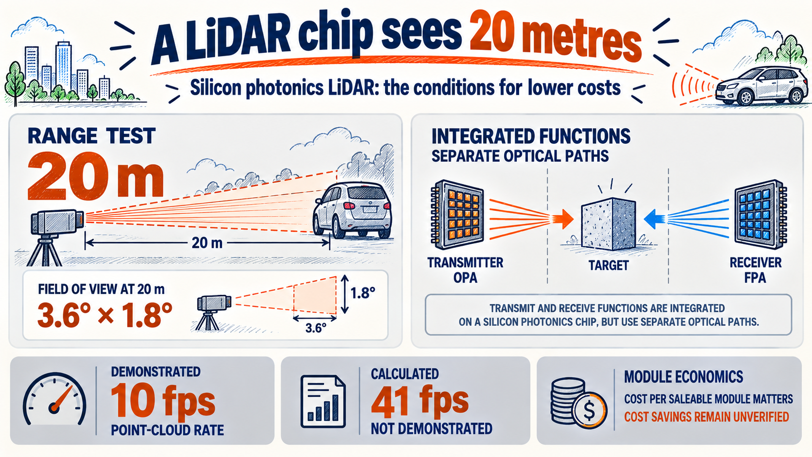
A silicon photonics LiDAR prototype has reconstructed a target 20 metres away. The research integrates the optical transmitter and receiver on one chip, suggesting a route to simpler sensor assembly. It does not establish a cheaper finished product. Understanding that distinction reveals both the engineering achievement and the business opportunity.
The work was published in Nature Communications on September 4, 2026, by researchers at imec and Tyndall. The available paper is a peer-reviewed, accepted article awaiting final editing. Experimental findings, industry evidence and the economic interpretation below have different levels of certainty. Primary source
What changes in silicon photonics LiDAR?
LiDAR sends light toward objects and uses the returning signal to locate them. Silicon photonics builds optical paths and components into a semiconductor chip. Its manufacturing appeal is the ability to fabricate many optical functions together rather than assemble every function separately. Primary source
FMCW, or frequency-modulated continuous-wave sensing, varies the frequency of a continuous laser signal. Comparing the return with reference light reveals range and motion toward or away from the sensor. That is radial velocity, not a complete measurement of motion in every direction. Primary source
Chip-based LiDAR already has a substantial research history. A 2022 Nature paper demonstrated silicon photonic LiDAR using microscopic mechanical switches. The new work should be judged by its transmitter–receiver architecture, rather than presented as the invention of LiDAR on a chip. Primary source
The transmitter is an optical phased array, or OPA, which steers light by controlling the relative phases of optical waves. The receiver is a focal-plane array, or FPA, behind a collecting lens. Separating the transmit and receive paths lets each perform a different job and removes the need for an optical circulator. Primary source
OPA transmitter
Steer the outgoing light
Job
Method · Control optical phase
FPA receiver
Collect and detect returns in parallel
Job
Method · Lens and detector array
The engineering idea is a division of labour. Efficient transmission and efficient collection do not necessarily demand the same optical geometry. Fabricating complementary functions together can relax a design compromise. Whether this also lowers cost is a separate manufacturing question.
Read the demonstration conditions before the headline numbers
The demonstrated point-cloud rate was 10 frames per second. A point cloud represents a scene as spatial coordinates. The 41 fps figure comes from a timing budget for an implementation that removes computer-side processing and transfer overhead. These are a measured result and a conditional projection, not two equivalent product benchmarks. Primary source
Not equivalent measurements. The 41 fps timing estimate assumes removal of computer-side bottlenecks. Source: paper pp.2,5.
The 20-metre test used a 3.6° by 1.8° field of view. A separate one-metre demonstration used 16° by 8°. Field of view describes how much of the scene the sensor covers. Combining the longer range and wider view into a single specification would misrepresent the experiments. Primary source
Near-range demonstration
1 m
Range
Field of view · 16° × 8°
Lens focal length · 8 mm
Longer-range demonstration
20 m
Range
Field of view · 3.6° × 1.8°
Lens focal length · 35 mm
The reported 3.7 mW is emitted optical power, not total electrical consumption. The prototype still needs a laser, processing electronics and thermal control. Its five-centimetre depth resolution is also not a guarantee of that accuracy on every surface and in every environment. Primary source
These distinctions matter to a buyer. If an aisle requires broad coverage but a sensor sees only a narrow area, the installation may need additional sensors or a different layout. A cheaper chip does not guarantee a cheaper deployed system. This is an economic implication of the experimental boundaries, not a result measured in the paper.
The cost question sits in assembly and testing
The paper is not a business case with a selling price or factory cost model. The economic analysis therefore starts with tasks that integration might remove, rather than an invented percentage cost reduction.
An optical module requires more than attaching parts. Optical paths must line up, and measurements must remain usable as conditions change. Defining some relative positions during chip fabrication could reduce repetitive alignment work during assembly. The saving would need to be demonstrated on a production line.
Integration also concentrates risk. A defect in one function can compromise a more valuable combined device. Yield is the share of manufactured devices that meet requirements. Poor yield or lengthy optical testing can consume the savings from simpler assembly.
-
1
Integrate optical functions
Define some relative positions during fabrication
-
2
Potentially simplify assembly
Measure actual alignment and connection savings
-
3
Account for yield and testing
Defects and calibration may offset savings
-
4
Compare cost per saleable module
Include deployment and maintenance
A meaningful quote includes packaging, calibration, testing and warranty costs per saleable module. Packaging connects and protects the chip. Calibration corrects differences between individual devices. Neither disappears simply because more optical functions have been integrated.
For Korean manufacturers, potential opportunities include automated optical alignment, thermal packaging and faster end-of-line inspection. This is not a revenue forecast for any named company. It identifies work a product developer would have to complete before shipping a dependable sensor.
Logistics offers a use case, not an automatic sales forecast
There is an existing application market. IFR’s World Robotics 2025 release recorded 102,900 transportation and logistics service robots sold in 2024, up 14%. Those figures come from a sample of 294 service-robot suppliers, not an estimate projected to the entire industry. Primary source
Multiplying that robot count by a sensor price would not establish this technology’s addressable market. Sensor counts vary, and existing machines can use cameras or other ranging systems. The competitor is the customer’s installed perception system, including its software and operating history.
A bounded logistics task looks like a plausible early validation setting. Routes and speeds can be constrained, allowing performance to be matched to a specific job. That is an inference, not evidence of a warehouse trial. Dark wrapping, shiny racks and occluded objects would still require field testing.
Productivity should be measured through unnecessary stops and human interventions, not sensor speed alone. Fewer interruptions could allow the same workforce and equipment to move more goods. Extra calibration or cleaning could reverse the benefit. The paper does not quantify either outcome.
A possible new market is smaller facilities that cannot justify today’s automation costs. That requires progress in safety engineering, site integration and maintenance as well as sensing. A more plausible displacement hypothesis is a shift from some discrete optical components and assembly tasks toward integrated modules and testing services, rather than wholesale replacement of existing LiDAR.
What the LG Innotek announcement does—and does not—show
A concrete investment example comes from Aeva’s July 29, 2025 announcement of a collaboration with LG Innotek. It described a package of up to approximately $50 million covering equity, product development and production capacity. This is evidence of an announced commitment, not verification that the entire amount has been spent. Primary source
The useful signal is that companies are allocating resources to manufacturing as well as sensing technology. Aeva’s commercial platform is separate from the imec research. The announcement does not establish adoption of this paper, a licence agreement or a commercial relationship with its authors. Primary source
The next commercial evidence should include detection performance under matched target and coverage conditions, saleable yield, testing time per module and downtime at customer sites. These measures reveal whether value accrues to chip designers, module makers or system operators.
This silicon photonics LiDAR expands the design options for combining transmission and reception. It offers a route toward simpler sensing hardware, while leaving the cost of that route unresolved. Alongside maximum range, watch the total expense of producing a working module and keeping it working in the field.
Sources were checked as of September 25, 2026. Company examples illustrate technology and industry structure; they are not recommendations to buy or sell securities.
Measure the cost of producing a working sensor module and keeping it working in the field.
Sources and further reading
For information only — this is not a recommendation to buy or sell any asset.
Comments 0