스크린 프린팅 페로브스카이트 태양전지 21.86% — 진짜 뉴스는 효율이 아니라 공정입니다Screen-Printed Perovskite Solar Cells at 21.86% — The Real News Is the Process, Not the Record
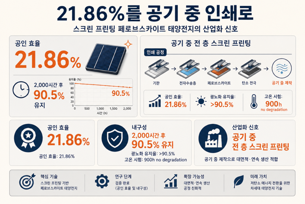
스크린 프린팅 페로브스카이트 태양전지는 2026년 8월 27일 Nature Photonics에 실린 논문 한 편으로 다시 주목받고 있습니다. 핵심은 21.86%라는 숫자 자체보다, 이 수치가 공기 중 인쇄 공정으로 나왔다는 점입니다.
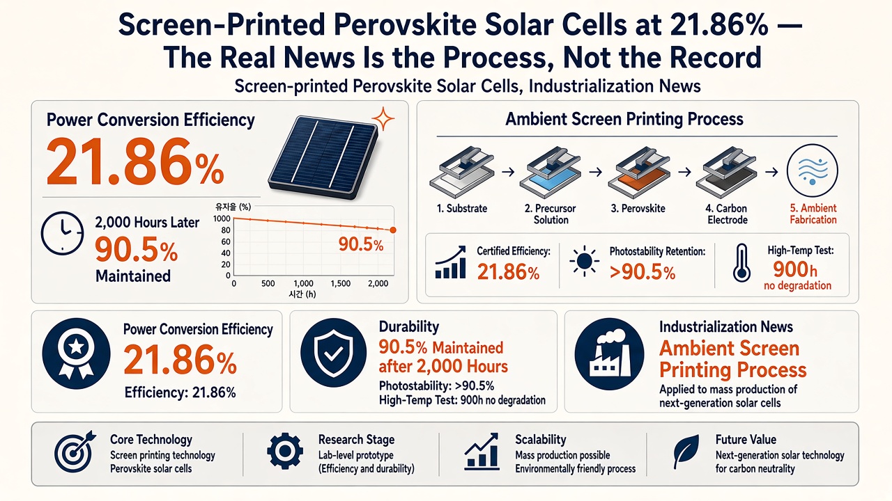
Screen-printed perovskite solar cells are back in focus because Nature Photonics published a notable paper on August 27, 2026. The important point is not just the 21.86% certified result. It is that the result came from an ambient-air printing route that looks much closer to factory logic than many earlier perovskite demonstrations.
스크린 프린팅 페로브스카이트 태양전지, 이번 연구가 왜 화제인가
연구진이 보고한 최고 효율은 22.41%, 외부 공인 효율은 21.86%였습니다. 실리콘 최고 기록을 갈아치운 것은 아닙니다. 그런데 공기 중에서 전 기능층을 스크린 프린팅으로 만들었다는 사실이 붙는 순간 이야기가 달라집니다. 실험실 전용 기술이 아니라 공장 라인 이야기로 넘어오기 때문입니다.
최근 몇 주 사이에도 Chem, Joule, Nature 계열에서 페로브스카이트 관련 결과가 여럿 나왔습니다. 그중 이번 논문을 고른 이유는 가장 단순합니다. 효율 자랑보다 제조 공정의 현실성을 더 많이 보여 준 논문이었습니다.
기존 기술과 무엇이 달랐나
페로브스카이트 태양전지는 오랫동안 같은 약점을 안고 있었습니다. 작은 셀에서는 성능이 잘 나오는데, 면적이 커지고 생산 환경이 거칠어지면 품질이 흔들린다는 점입니다. 그래서 높은 효율을 보여 준 많은 연구가 진공 장비나 불활성 분위기, 다시 말해 공장에 바로 들이기엔 부담이 큰 조건에 기대 왔습니다.
이번 연구는 그 병목을 정면으로 겨눴습니다. 연구진은 메틸암모늄 프로피오네이트와 부티로니트릴을 섞은 공용매로 잉크의 흐름과 결정 성장을 함께 제어했습니다. 말이 어렵지만 요지는 분명합니다. 잉크가 두꺼운 다층 구조 안쪽까지 더 깊게 스며들고, 결정이 표면에서 먼저 엉키지 않도록 만들어 결함을 줄였다는 뜻입니다. 그 결과 탄소 전극과의 접촉도 좋아졌습니다.
기존 고성능 실험실형
환경 · 진공·불활성 분위기 의존이 큼
공정 · 여러 섬세한 증착·코팅 단계
병목 · 대면적 균일성·수율
산업화 느낌 · 성능은 좋지만 공장 전환이 어려움
이번 인쇄형 공정
환경 · 공기 중 전 층 스크린 프린팅
공정 · 잉크 흐름과 결정 형성을 함께 제어
병목 대응 · 깊은 침투·결함 억제·전극 접촉 개선
산업화 느낌 · 기존 인쇄 생태계와 연결 가능
숫자로 보면 어디까지 왔나
논문에서 확인된 사실은 꽤 강합니다. 소자는 22.41% 효율을 기록했고, 외부 공인 수치도 21.86%였습니다. 내구성도 눈에 띕니다. ISOS-L-1(국제 표준 가속 노화 시험) 조건에서 2,000시간 뒤에도 초기 효율의 90.5% 이상을 유지했고, 85도와 상대습도 50% 안팎의 ISOS-L-3 조건에서는 900시간 작동 후 열화가 없었다고 보고했습니다.
물론 이 데이터를 바로 상업화 완료 신호로 읽으면 과장입니다. 여기까지는 논문 실험 조건에서 검증된 셀 수준 결과입니다. 대형 모듈이 야외에서 몇 년을 버티는지, 금융기관이 프로젝트 파이낸싱을 붙일 만큼 신뢰할 수 있는지는 아직 다른 문제입니다. 그래도 페로브스카이트가 늘 듣던 비판, 즉 효율은 좋은데 오래 못 버틴다는 말에는 분명한 반박이 생겼습니다.
중국 대비 지역별 태양광 제조 비용 격차를 보여 주는 막대그래프. IEA 자료를 바탕으로 중국을 100으로 둔 상대 비교입니다. 인도 약 110, 미국 120, 유럽 135 수준입니다.
왜 이게 제조비용을 낮출 수 있나
태양광에서 비용은 재료값만으로 결정되지 않습니다. 장비 가격, 공정 수, 수율, 불량률, 생산 속도, 환경 제어 부담이 모두 돈입니다. 미국 에너지부는 페로브스카이트가 저온 공정과 잉크 기반 프린팅 덕분에 공정을 줄이고 자본 부담도 낮출 잠재력이 있다고 설명합니다. NREL은 단일접합 페로브스카이트 모듈의 최소지속가능가격을 와트당 0.38달러, 장기적으로는 0.18달러까지 낮출 수 있다고 추정했습니다.
이번 논문이 중요한 이유는 그 잠재력을 더 구체적인 제조 경로로 보여 줬기 때문입니다. 고가의 진공 증착 장비를 덜 쓰고, 글러브박스 같은 까다로운 환경 의존도를 낮추고, 업계가 이미 익숙한 인쇄 공정을 더 많이 활용할 수 있다면 CAPEX(초기 설비투자비)와 라인 전환 부담이 함께 내려갈 수 있습니다. 논문이 정확한 절감률을 계산해 준 것은 아니므로, 여기서부터는 전망이 섞입니다. 다만 비용이 왜 내려갈 수 있는지는 이제 훨씬 설명하기 쉬워졌습니다.
-
1
논문 사실
공기 중 인쇄로 21.86% 공인 효율
-
2
제조 의미
공정 단순화와 장비 선택지 확대
-
3
비용 경로
설비투자·불량률·라인 속도 개선 여지
-
4
산업 효과
신규 업체 진입과 제품 형태 다변화
-
5
시장 결과
설치 면적당 전력 증가 또는 새 수요 창출
인쇄 공정이 열어 주는 세 갈래 기회
첫 번째 기회는 상업화 업체입니다. Oxford PV는 2024년 9월 미국 고객에게 세계 최초의 상업용 페로브스카이트-실리콘 탠덤 패널 출하를 발표했고, 2026년 6월에는 Fraunhofer ISE와 함께 25.6% 모듈 효율 설계를 공개했습니다. 즉, 산업은 이미 실험실 이후 단계로 한 발 들어가 있습니다. 이번 논문은 그 흐름에 “인쇄형 단일접합”이라는 또 다른 제조 카드가 추가될 수 있음을 보여 줍니다.
장비·소재 생태계에도 변화가 생깁니다. 인쇄식 공정이 커지면 잉크, 용매, 기판, 스크린 장비, 건조 장비, 봉지(encapsulation) 기술의 중요도가 올라갑니다. 반대로 진공 장비 중심으로만 밸류체인을 짜 두었던 업체는 다시 계산해야 할 수 있습니다. 이 변화는 기존 산업을 하루아침에 없애는 그림보다는, 어디에서 부가가치가 붙는지가 달라지는 그림에 가깝습니다.
새 시장을 여는 카드도 있습니다. 페로브스카이트는 얇고 가볍게 만들 수 있어 건물일체형 태양광(BIPV), 경량 모듈, 휴대형 전원, 곡면 설치 같은 영역과 잘 맞습니다. 경제적으로 중요한 질문도 여기 있습니다. 실리콘을 전부 대체하느냐보다, 같은 면적에서 더 많은 전기를 만들거나 기존 패널이 못 들어가던 장소에서 새 수요를 만들 수 있느냐가 더 현실적인 승부처입니다.
대면적 수율부터 은행가능성까지 — 아직 남은 숙제
남은 과제도 분명합니다. 미국 에너지부가 반복해서 짚는 지점은 안정성, 대면적 성능 유지, 제조 재현성, 그리고 은행가능성(bankability, 금융기관이 프로젝트에 대출·보험을 붙일 수 있는 정도)입니다. 한 장의 셀에서 잘 나오는 것과 수천 장 모듈이 같은 품질로 나오는 것은 완전히 다른 문제입니다. 결국 공장에서의 수율과 야외 장기 데이터가 쌓여야 금융도 따라옵니다.
- 논문이 증명한 사실: 공기 중 전 층 스크린 프린팅으로 21.86% 공인 효율과 개선된 내구성을 보였습니다.
- 아직 검증이 필요한 부분: 대형 모듈 수율, 장기 야외 성능, 실제 생산라인의 비용 구조입니다.
- 전망의 영역: 기존 실리콘 공정과 설비를 얼마나 재활용할 수 있는지, 그리고 LCOE(균등화발전비용, 1kWh를 만드는 데 드는 평생 평균 비용)가 얼마나 내려갈지는 후속 데이터가 더 필요합니다.
- 다만 이 연구가 특정 기업의 실적 개선이나 주가 상승을 직접 보장하는 신호는 아닙니다.
논문 한 편이 바꿀 수 있는 것, 아직 못 바꾸는 것
이번 Nature Photonics 논문의 진짜 의미는 효율 기록 하나가 아닙니다. 페로브스카이트 태양전지가 좋은 실험을 넘어, 실제 공장 공정으로 갈 수 있다는 경로를 조금 더 또렷하게 그렸다는 데 있습니다. 이 경로가 공장 수율과 장기 신뢰성으로 이어지면 태양광 산업은 더 낮은 설비 부담, 더 다양한 제품 형태, 그리고 새로운 설치 시장을 얻게 될 수 있습니다. 반대로 그 검증이 실패하면 이번 결과도 훌륭한 논문으로만 남습니다. 2026년 9월 4일 지금 시점에서 중요한 것은 기록 경쟁이 아니라, 이 공정이 정말 공장에서도 반복되느냐입니다.
중요한 숫자는 21.86%만이 아닙니다. 공장이 이미 아는 방식으로 고효율 태양전지를 만들 수 있다는 가능성입니다.
출처
- Nature Photonics: Fluid motion and crystallization control enable air-processed fully screen-printed perovskite solar cells
- DOE: Perovskite Solar Cells
- DOE: Perovskite Research Directions
- NREL: PV and PV-Plus-Storage Cost Declines
- IEA: Energy Technology Perspectives 2026
- IEA: Solar PV Global Supply Chains
- Oxford PV first commercial tandem shipment
- Oxford PV and Fraunhofer ISE collaboration
- HZB / EurekAlert: evaporated perovskites in tandem solar cells improved
- Chem / EurekAlert: scalable production of high-efficiency perovskite solar cells
Why this screen-printed perovskite solar cell paper matters
The device reached 22.41% efficiency, with a certified value of 21.86%. That does not overturn the best silicon records. What changes the story is that every functional layer was screen-printed in air. Once that detail enters the picture, this stops being only a lab-efficiency story and starts looking like a manufacturing story.
Recent weeks also brought perovskite advances in Chem and Joule. I chose this paper because it answered the factory question more directly than the others. It was the clearest recent paper showing how perovskites might move from a lab result to a repeatable production route.
What changed versus earlier perovskite work
Perovskite solar cells have long carried the same warning label: excellent small-cell efficiency, limited confidence in large-scale manufacturing. The material is sensitive to moisture, hard to coat uniformly over larger areas, and vulnerable to defects that quickly damage performance. That is why many high-performance devices still rely on vacuum tools or tightly controlled inert environments.
This paper goes straight after that bottleneck. The researchers used a co-solvent system of methylammonium propionate and butyronitrile to control fluid motion and crystal growth together. In practical terms, the ink penetrated the multilayer structure more deeply, crystals formed in a more orderly bottom-up way, defects were suppressed, and contact with the carbon electrode improved.
Earlier high-performance lab route
Environment · Heavy reliance on vacuum or inert environments
Process · Multiple delicate deposition and coating steps
Bottleneck · Large-area uniformity and yield
Industrial feel · Strong performance, harder factory transfer
This printed route
Environment · All layers screen-printed in ambient air
Process · Controls ink flow and crystallization together
Bottleneck response · Deeper infiltration, fewer defects, better electrode contact
Industrial feel · Potentially closer to existing printing ecosystems
How far the numbers have moved
The hard facts in the paper are meaningful. The device reached 22.41% efficiency, with a certified 21.86%. It also retained more than 90.5% of its initial efficiency after 2,000 hours under the ISOS-L-1 accelerated aging protocol, and showed no degradation after 900 hours of operation at 85C and about 50% relative humidity under ISOS-L-3 conditions.
That still does not mean commercialization is finished. These are cell-level results under defined test conditions, not proof of multi-year outdoor module performance. But they do answer one of the field’s oldest criticisms: perovskites often looked efficient long before they looked durable.
Bar chart showing regional solar manufacturing cost gaps versus China. Based on IEA framing with China normalized to 100. India is about 110, the United States 120, and Europe 135.
Why this could lower manufacturing costs
In solar manufacturing, cost is not just the materials bill. It also comes from equipment, process complexity, yield loss, line speed, and environmental control. The U.S. Department of Energy says perovskites have low-cost potential because low-temperature, ink-based processing could reduce the number and price of manufacturing steps. NREL estimated a minimum sustainable price of $0.38 per watt for small-scale single-junction perovskite modules, with longer-term projections down to $0.18 per watt.
This paper matters because it makes that cost story easier to believe. If manufacturers can rely less on expensive vacuum deposition, less on glovebox-style production, and more on printing workflows the industry already knows, capital expenditure (CAPEX) and line-conversion burdens could fall together. The paper does not calculate a precise savings number, so that part remains an inference. Still, the path from materials science to factory economics is much clearer now.
-
1
Paper fact
21.86% certified efficiency in ambient-air printing
-
2
Manufacturing implication
Simpler processing and broader equipment choices
-
3
Cost path
Potential relief on capex, defects, and line speed
-
4
Industry effect
Easier entry and more product formats
-
5
Market result
More power per area or new demand creation
Three opportunities the printing route opens up
The first opportunity is for commercialization players. Oxford PV announced the first commercial shipment of perovskite-silicon tandem panels to a U.S. customer on September 5, 2024, and in June 2026 it presented a 25.6% efficient module design with Fraunhofer ISE. Industry has already moved beyond the pure-lab stage. This paper adds another possible production route to that transition.
The equipment and materials ecosystem would also change. If printing-based processes expand, inks, solvents, substrates, screen tools, drying systems, and encapsulation technologies all become more strategically important. That would not erase vacuum-heavy supply chains overnight, but it could change the equipment mix and shift where value is captured.
There is also a new-market angle. Perovskites can be thin and lightweight, which makes them interesting for building-integrated photovoltaics, lightweight modules, portable power, and curved surfaces. The real business question is not whether they replace all silicon. It is whether they can generate more electricity from the same area, or create installations conventional modules struggle to serve.
From large-area yield to bankability, the hard part is still ahead
Major constraints remain. DOE keeps returning to the same four ideas: durability, efficiency at scale, manufacturability, and bankability, meaning whether lenders and insurers will back a project on reasonable terms. A beautiful cell result and a repeatable commercial module are not the same product. Factory yield and long outdoor validation are what ultimately bring financing with them.
- What the paper established: certified 21.86% efficiency and stronger durability with an ambient, fully screen-printed route.
- What still needs proof: module-scale yield, long outdoor lifetime, and real factory cost structure.
- What remains inference: how much existing silicon know-how can be reused, and how far LCOE, or levelized cost of electricity, can actually fall.
- This is not a direct forecast for any one company’s earnings or stock performance.
The real breakthrough is a factory path, not a record
The core significance of this Nature Photonics paper is not the headline efficiency number by itself. It is that perovskite solar cells may be getting a more believable factory path. If that path survives scale-up and long-term validation, the economic effects could include lower upfront equipment burden, more product formats, and new end markets. If it fails, this remains an impressive paper rather than an industrial turning point. As of September 4, 2026, that is the line that matters.
The important number is not just 21.86%. It is the possibility that a high-efficiency solar cell can be made with a process factories already understand.
Sources
- Nature Photonics: Fluid motion and crystallization control enable air-processed fully screen-printed perovskite solar cells
- DOE: Perovskite Solar Cells
- DOE: Perovskite Research Directions
- NREL: PV and PV-Plus-Storage Cost Declines
- IEA: Energy Technology Perspectives 2026
- IEA: Solar PV Global Supply Chains
- Oxford PV first commercial tandem shipment
- Oxford PV and Fraunhofer ISE collaboration
- HZB / EurekAlert: evaporated perovskites in tandem solar cells improved
- Chem / EurekAlert: scalable production of high-efficiency perovskite solar cells
이 글은 정보 제공 목적이며, 특정 자산의 매수·매도를 권유하지 않습니다.
For information only — this is not a recommendation to buy or sell any asset.
댓글Comments 0