Quantum memory: could an 8-bit design lower hardware costs? (Views 2)
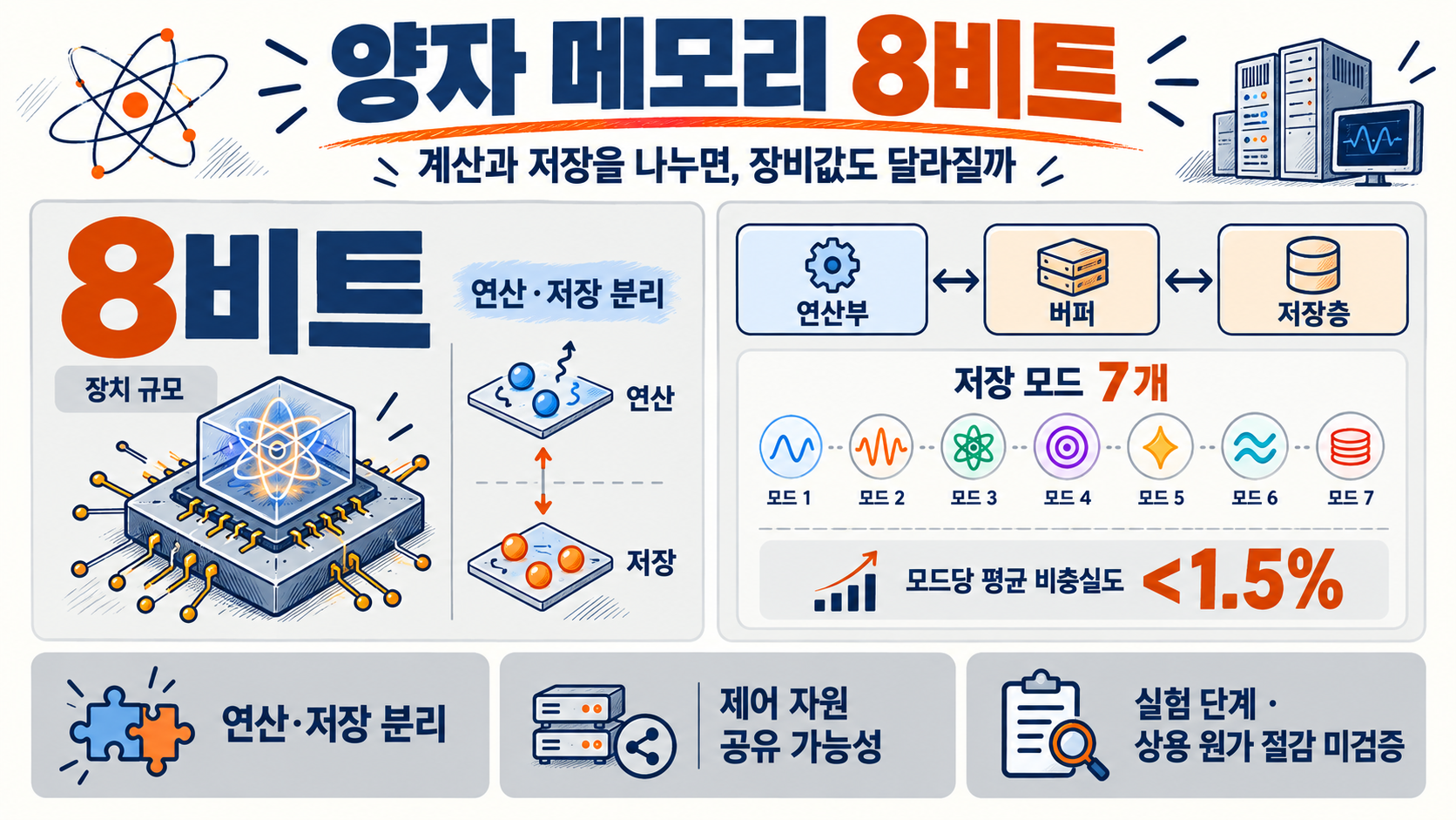
An eight-bit quantum memory experiment points toward separating computation from storage. Published in Nature Physics on September 8, 2026, it raises a practical question: could a small memory module help make a larger quantum computer less expensive? Nature Physics 정식 논문
For readers used to laptop storage, eight bits will sound small. The interesting feature is how one processing unit serves several storage locations. Separating preservation from computation lets engineers design each part around its own requirements. Source
The first preprint appeared in March 2025, followed by journal publication in September 2026. The researchers demonstrated memory operation and control performance. Commercial cost savings still need testing; the economic discussion here assumes that the technology can scale. Source
Why separate quantum memory from the processor?
A qubit can produce a zero or a one when measured, but its computation also depends on preserving relationships between quantum states. Unwanted interactions disturb those relationships. Storing quantum information therefore requires more than retaining a readable classical value. Source
Processing needs controllable interactions; storage benefits from remaining undisturbed. The public manuscript separates these conflicting requirements. That gives engineers a way to improve the processing and storage subsystems independently. Source
A buffer sits between the transmon, a superconducting circuit, and the storage cavity. The cavity holds electromagnetic modes—distinct patterns of oscillation. A selected mode exchanges its quantum state with the buffer, which provides access to the processor. Source
Quantum memory access path
FlowStates swap in both directions. Addressing is classical. Original schematic based on manuscript Fig. 1.
Random access means choosing storage locations in an arbitrary order. Selection uses classical control. It is distinct from QRAM with coherent quantum addressing, and does not demonstrate reading all data at once or accelerating AI training. Source
Eight bits and seven storage modes need different labels
The published abstract describes an eight-bit device and seven addressable storage modes served by one transmon. The manuscript distinguishes the buffer from the storage bank. Eight independent storage modes would be an inaccurate description of the published result. Source
The reported average infidelity is below 1.5% per mode. Infidelity measures departure from the intended quantum operation. It is not the failure probability of an entire computer or a long algorithm; repeated operations need a separate assessment. Source
The manuscript also examines unwanted interactions among modes. Scaling capacity introduces interactions that must be controlled, not just extra places to store information. A small-module result cannot simply be multiplied into a large-system forecast. Source
The potential saving is in control resources
If every additional storage location requires a matching set of processing and control resources, expansion becomes expensive. Sharing those resources could reduce how much new equipment each increment of capacity needs.
Fewer duplicated components would not automatically mean a cheaper purchase. Buffers, cavities and couplers add fabrication and testing costs. Assembly and calibration also matter. A shared component that disables several locations when it fails could trade component savings for lower manufacturing yield.
Operators face another trade-off. Sharing a processor can create access queues and reduce throughput. Preserving idle states and moving them only when needed could instead improve resource use. The balance depends on the workload and error-correction schedule.
A more useful comparison is total cost per completed computation at the same accuracy. It combines equipment depreciation, operation and control costs, then relates them to useful completed work. The evidence reviewed here does not establish that commercial cost comparison.
Conditions for lower computation cost
FlowConditional editorial analysis, not measured cost savings from the paper.
For example, a lower purchase price can coexist with a higher cost per job if processing slows too much. A more expensive machine can be economical if it avoids enough failed work. These are explanatory cases, not measured outcomes from this experiment.
Other technologies face the same need to connect laboratory performance with manufacturing economics. Our article on solid-state battery electrolyte films examines the conditions for lower manufacturing costs. Quantum memory likewise needs performance and production and operating costs assessed together. 전고체 배터리 전해질 막 — 제조비 절감의 조건
What roadmaps and funding actually tell us
IBM’s roadmap targets 200 logical qubits and 100 million gates for Starling in 2029. Logical qubits are information units protected by error correction; gates are elementary operations on quantum states. IBM 공식 로드맵
IBM presents these figures as future targets. They should not be read as delivered performance or an announcement that it will adopt this memory. The roadmap shows why efficient allocation of storage and control resources matters as systems grow.
Honeywell announced an approximately $600 million Quantinuum funding round in September 2025 at a $10 billion pre-money valuation. Participants included NVentures and Korea Investment Partners. This was a historical financing announcement, not a current valuation or an estimate of the entire quantum market. Honeywell 자금조달 발표
That financing cannot be turned into revenue for this research. The experiment and the funded company are not the same business. Investment in the sector still leaves product qualification and customer contracts between a promising design and commercial demand.
A possible market for modules and control, not a DRAM replacement
If commercialization advances, likely early customers would be quantum-system builders and research institutions. They would evaluate access time, errors and control costs in their own systems. Comparable qualification methods and interfaces would make independent suppliers easier to assess.
Possible product categories include qualified memory modules, precision coupling components and software that schedules access. Adoption might reduce demand for some duplicated control resources. These are conditional business possibilities, not identified winners or booked sales.
The paper acknowledges research support from the Samsung Advanced Institute of Technology. Research support is not a production contract or product commitment, so it cannot be treated as evidence of future memory revenue. Source
This device is not a direct replacement for PC DRAM or AI-accelerator HBM. It stores a different kind of information for a different system. Existing manufacturing experience may help, but product specifications and customer qualification would still have to be established.
The conventional AI-chip supply chain offers a useful comparison for how processing, memory and packaging fit together. Before borrowing that market’s size for quantum memory, identify the function the customer is actually buying. H200 한 장, 31곳 — AI 칩 공급망 해설
Beyond eight bits: scale, error correction and economics
The next questions concern scale and protected operation. More storage locations and modules must remain manageable in both access error and latency. Long computations also need error correction integrated with the storage schedule.
The third question is economic: compare complete systems using the same workload, accuracy and operating conditions. A cheaper bill of materials is not enough if completing the job costs more. Until these tests exist, translating eight bits into revenue or a savings percentage would be premature.
The meaningful change is a more concrete route to optimizing quantum processing and storage separately. Industrial value would follow if that delivered more useful computation with fewer additional control resources. Future demonstrations should report the resources needed to finish the work alongside qubit counts.
Sources were reviewed as of September 18, 2026. This article uses the published abstract and funding statement, the public manuscript and official company disclosures. Published abstract figures take precedence over preprint wording. It is technology and industry analysis, not a recommendation to buy or sell securities.
Judge quantum memory economics by the resources needed to complete a computation at equal accuracy.
Sources and further reading
양자 메모리 8비트, 양자컴퓨터 장비값을 줄일 수 있을까 (조회수 2)
양자 메모리 8비트 실험이 계산하는 회로와 정보를 보관하는 공간을 분리하는 길을 보여줬습니다. 9월 8일 Nature Physics에 실린 연구입니다. 작은 저장장치가 왜 양자컴퓨터의 장비값과 연결되는지, 실제 성과와 사업화 조건을 나눠 짚어봅니다. Nature Physics 정식 논문
노트북의 저장 용량에 익숙한 독자라면 8비트라는 숫자가 작게 느껴질 것입니다. 이번 실험에서 눈여겨볼 부분은 연산부 하나가 여러 저장 공간을 다루는 구조입니다. 양자 정보를 오래 보관하는 일과 필요할 때 꺼내 계산하는 일을 나눠 맡기면, 각각에 맞는 장치를 설계할 수 있습니다. 근거 자료
첫 공개 원고는 2025년 3월에 나왔고, 2026년 9월 정식 논문으로 게재됐습니다. 연구팀이 보여준 것은 메모리의 작동과 제어 성능입니다. 상용 컴퓨터의 원가가 얼마나 내려가는지는 후속 검증이 필요하며, 이 글의 비용·시장 전망도 기술이 확장될 경우를 가정한 분석입니다. 근거 자료
양자 메모리는 왜 연산부와 떨어져 있어야 할까
양자컴퓨터가 다루는 정보 단위는 큐비트입니다. 일반 비트처럼 0이나 1을 읽을 수 있지만, 계산 중에는 두 상태 사이의 섬세한 관계도 유지해야 합니다. 주변 환경과 원치 않게 상호작용하면 그 관계가 흐트러집니다. 단순히 데이터를 저장해 두고 나중에 읽으면 되는 문제가 아닙니다. 근거 자료
계산할 때는 상태를 바꾸기 쉽도록 회로 사이의 상호작용을 활용합니다. 반대로 오래 저장하려면 불필요한 상호작용을 줄여야 합니다. 공개 원고는 이 두 요구를 서로 다른 부분이 맡게 하는 구조를 설명합니다. 연산에 알맞은 장치와 보존에 알맞은 장치를 각각 개선할 수 있다는 점이 과학·공학적 의미입니다. 근거 자료
연구팀은 트랜스몬이라는 초전도 회로와 저장 공간 사이에 버퍼를 넣었습니다. 버퍼는 정보를 잠시 받아 전달하는 중간 공간입니다. 저장 공간은 전자기파를 가두는 공진기이며, 서로 다른 진동 방식인 모드를 이용합니다. 필요한 모드를 골라 버퍼와 상태를 교환하는 방식입니다. 근거 자료
양자 메모리의 접근 경로
흐름도상태는 양방향으로 교환합니다. 주소 선택은 고전적 제어입니다. 공개 원고 Fig.1 기반 자체 도식.
여기서 랜덤 액세스는 저장 위치를 임의의 순서로 선택할 수 있다는 뜻입니다. 주소 자체를 양자 중첩으로 다루는 QRAM과는 구별해야 합니다. 이 실험의 주소 선택은 고전적 제어로 이뤄집니다. 모든 데이터를 한 번에 읽거나 AI 학습을 즉시 가속했다는 의미는 아닙니다. 근거 자료
8비트와 7개 저장 모드, 숫자를 나눠 읽어야 합니다
정식 논문은 장치를 8비트 메모리로 소개하고, 단일 트랜스몬이 주소를 지정하는 저장 모드는 7개라고 명시합니다. 공개 원고의 구조는 버퍼와 저장층을 나눠 보여줍니다. 따라서 저장 모드 8개를 독립적으로 제어했다고 옮기면 정확하지 않습니다. 근거 자료
정식 초록에 제시된 모드당 평균 비충실도는 1.5% 미만입니다. 비충실도는 의도한 양자 동작에서 얼마나 벗어났는지를 나타내는 지표입니다. 이를 컴퓨터 전체의 고장률이나 긴 계산의 실패 확률로 바꿔 읽을 수는 없습니다. 작동을 많이 반복할 때의 누적 오류는 별도로 확인해야 합니다. 근거 자료
공개 원고는 다른 저장 모드 사이의 상호작용이 오류를 만들 수 있다는 점도 다룹니다. 저장 공간을 늘리면 용량만 늘어나는 것이 아니라 관리할 상호작용도 늘어납니다. 실험실의 작은 모듈에서 얻은 결과를 대규모 시스템에 그대로 곱할 수 없는 이유입니다. 근거 자료
비용 절감의 핵심은 저장 공간보다 제어 장비입니다
저장 공간이 늘어날 때마다 별도의 연산·제어 자원을 똑같이 붙여야 한다면 시스템 비용도 함께 커집니다. 여러 저장 위치가 제어 자원을 공유할 수 있다면 장비를 추가하는 속도를 늦출 여지가 생깁니다. 연구가 비용 문제와 만나는 지점입니다.
그러나 부품 수를 줄였다는 사실만으로 구매 가격이 낮아지지는 않습니다. 버퍼·공진기·연결 장치를 만들고 검사하는 비용이 추가됩니다. 시스템 조립과 보정에 드는 시간도 봐야 합니다. 특히 공통 부품 하나의 결함으로 여러 저장 위치를 함께 쓸 수 없게 된다면, 부품을 적게 쓰는 이점이 수율 손실로 사라질 수 있습니다.
운영자의 계산은 더 까다롭습니다. 하나의 연산부를 함께 쓰느라 접근 대기가 길어지면 같은 시간에 끝내는 작업이 줄어들 수 있습니다. 반대로 충분히 오래 보관하면서 필요한 정보만 옮길 수 있다면 비싼 연산부를 더 효율적으로 배치할 수 있습니다. 어느 쪽이 큰지는 실행할 알고리즘과 오류 보정 방식에 달려 있습니다.
그래서 비교해야 할 값은 저장 위치 하나의 가격보다, 같은 정확도로 계산 하나를 끝내는 총비용입니다. 장비 감가상각과 유지비, 제어 비용을 더하고 성공적으로 끝낸 유효 작업 수로 나누는 접근입니다. 이 논문에서 그런 상업적 비용 비교가 입증됐다고 주장할 근거는 없습니다.
장비 절약이 계산 비용 절감으로 이어지는 조건
흐름도편집부의 조건부 경제 분석입니다. 논문의 실측 원가 절감 결과가 아닙니다.
가령 장비 구입비가 내려가더라도 처리 시간이 더 크게 늘어난다면 작업당 비용은 오를 수 있습니다. 반대로 구매 가격이 조금 높아도 오류 때문에 다시 계산하는 횟수가 크게 줄면 경제성이 좋아질 수 있습니다. 이 예시는 방향을 설명하기 위한 것으로, 이번 연구의 실측 손익을 계산한 결과는 아닙니다.
실험 성과를 제조비와 연결할 때 이런 검증은 다른 기술에서도 필요합니다. 전고체 배터리 전해질 막을 다룬 글도 성능 개선이 실제 제조비 절감으로 이어질 조건을 살펴봅니다. 양자 메모리 역시 장치의 성능과 생산·운영 비용을 함께 비교해야 합니다. 전고체 배터리 전해질 막 — 제조비 절감의 조건
기업의 로드맵과 투자금은 무엇을 말해주나
산업에서는 이미 오류를 줄여 장시간 계산하는 시스템을 목표로 내세우고 있습니다. IBM의 공식 로드맵은 2029년 Starling에 논리 큐비트 200개와 1억 회의 게이트 연산을 제시합니다. 논리 큐비트는 오류 보정을 통해 보호하는 정보 단위이고, 게이트는 양자 상태를 바꾸는 기본 연산입니다. IBM 공식 로드맵
IBM이 제시한 수치는 앞으로 달성하려는 목표입니다. 현재 성능이나 이번 메모리의 채택 발표로 읽어서는 안 됩니다. 이 로드맵에서 눈여겨볼 대목은 큰 시스템을 만들수록 저장·제어 자원을 효율적으로 배치하는 일이 개발 과제가 된다는 점입니다.
투자 규모의 사례도 있습니다. Honeywell은 2025년 9월 Quantinuum이 약 6억 달러를 조달한다고 발표했습니다. 투자 전 기업가치 평가는 100억 달러였고, NVentures와 한국투자파트너스도 참여자에 포함됐습니다. 이것은 특정 시점의 자금조달 발표이지 현재 기업가치나 양자컴퓨팅 전체 시장 규모가 아닙니다. Honeywell 자금조달 발표
이 투자 사례를 논문 기업의 매출로 연결하면 안 됩니다. 연구팀의 장치와 투자받은 기업은 같은 사업이 아닙니다. 자본이 이 분야에 들어온다는 사실과 특정 메모리 설계가 고객을 확보한다는 사실 사이에는 제품 검증과 구매 계약이라는 단계가 남아 있습니다.
새 시장은 모듈·제어에서, 기존 DRAM 대체는 별개입니다
사업화가 진행된다면 초기 고객은 일반 소비자보다 양자컴퓨터를 만드는 기업과 연구기관일 가능성이 높습니다. 이들은 저장 용량이라는 숫자만 사는 것이 아니라, 자기 연산부에 연결했을 때의 오류·접근 시간·제어 비용을 함께 평가할 것입니다. 표준화된 시험 방법과 연결 규격이 있어야 공급업체를 비교하기도 쉬워집니다.
여기서 새 시장이 생긴다면 고품질 저장 모듈, 정밀 연결 부품, 접근 순서를 관리하는 제어 소프트웨어가 후보입니다. 반면 저장 위치마다 제어 자원을 많이 붙이는 설계의 일부 수요는 줄어들 수 있습니다. 이는 채택이 이뤄진다는 조건 아래의 전망이며, 특정 기업의 수혜를 확인한 결과는 아닙니다.
국내와의 연결도 과장할 필요는 없습니다. 정식 논문은 삼성종합기술원의 연구 지원을 명시합니다. 하지만 연구 지원은 양산 계약이나 제품 탑재와 다릅니다. 이 사실만으로 삼성의 메모리 매출에 기여한다고 계산할 수 없습니다. 근거 자료
양자 상태를 보관하는 이 장치는 PC의 DRAM이나 AI 가속기의 HBM을 바로 대체하는 제품도 아닙니다. 저장하는 정보와 연결할 시스템이 다릅니다. 기존 메모리 업체의 제조 경험이 도움이 될 여지는 있어도, 제품 규격과 고객 검증을 새로 통과해야 합니다.
일반 AI 칩에서 연산·메모리·패키징이 어떤 공급망을 이루는지 비교하면 차이를 이해하기 쉽습니다. 양자 메모리에 기존 반도체의 시장 규모를 그대로 붙이기 전에, 고객이 사려는 기능부터 구분해야 합니다. H200 한 장, 31곳 — AI 칩 공급망 해설
확장성·오류보정·경제성 — 8비트 이후의 세 가지 숙제
첫째는 확장성입니다. 저장 위치와 모듈을 늘려도 접근 오류와 대기 시간이 감당할 수준인지 확인해야 합니다. 둘째는 오류 보정을 포함한 전체 동작입니다. 정보를 보관하는 중에도 보호 절차를 수행할 수 있어야 오래 걸리는 계산에 쓸 수 있습니다.
셋째는 경제성 비교입니다. 같은 작업, 같은 정확도, 같은 운영 조건에서 기존 구성과 비용을 비교해야 합니다. 부품 목록만 저렴한지, 실제 계산을 마치는 데 드는 비용도 낮은지 나눠 봐야 합니다. 이 세 가지가 확인되기 전까지 8비트를 대규모 매출이나 특정 절감률로 환산하기는 어렵습니다.
이번 연구에서 읽을 변화는 양자컴퓨터에도 계산과 저장을 따로 최적화하는 설계가 구체화된다는 점입니다. 제어 장비를 덜 늘리면서 유용한 계산을 더 많이 할 수 있다면 산업적 가치가 생깁니다. 다음 성과 발표에서는 큐비트 개수와 함께 그 계산을 끝내는 데 필요한 자원도 보고 싶습니다.
자료 확인 기준일은 2026년 9월 18일입니다. 정식 논문의 공개 초록과 연구비 항목, 공개 원고, 기업 공식 자료를 사용했습니다. 구조 설명은 공개 원고를 보완 자료로 삼았고 수치는 정식 초록을 우선했습니다. 이 글은 기술·산업 분석이며 특정 종목의 매수·매도 권유가 아닙니다.
양자 메모리의 경제성은 같은 정확도의 계산을 끝내는 데 필요한 자원으로 판단해야 합니다.
답글 남기기