K153 High-Index Polymer at 2.53 — The First Test for Replacing Glass Optics with Film (Views 0)
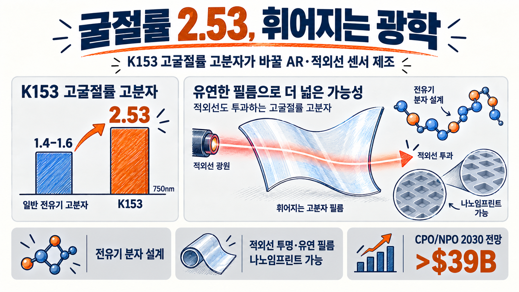
The K153 high-index polymer tackles a stubborn weakness of plastic optics. In a Nature Photonics paper published on September 10, 2026, its refractive index reached about 2.53 at 750 nanometers—well above the typical 1.4–1.6 range for all-organic polymers and above 2.25 for the selected inorganic comparators in the paper. Here is where that number comes from and what it must still prove on a factory floor.
This sounds like a story about a plastic that bends light. The industrial question is more concrete. High-performance lenses and waveguides often rely on glass, silicon or compound semiconductors that are rigid and demanding to process. If similar optical strength can be placed in a flexible film and patterned by nanoimprint, component count, alignment and assembly costs could change.
One distinction matters here: the paper demonstrates a material and prototype functions. It does not report adoption in smart glasses or data-center photonics. Refractive index, transparency and process demonstrations below are research results; cost reductions and market effects are conditional outlooks. This article does not recommend buying or selling any company or security mentioned.
K153 high-index polymer: what does 2.53 mean?
Refractive index measures how much light slows and changes direction inside a material. A higher value gives a material more influence over light within the same distance. A lens can focus more strongly, while a waveguide can confine light more tightly.
In practical devices, larger index contrast can reduce leakage at boundaries and allow tighter bends. That connects refractive index to lens thickness, the field of view in AR glasses and the footprint of photonic circuits.
Refractive index at 750 nm
DataValues cited in the abstract; not a comparison with every inorganic material.
Conventional polymers are light, flexible and moldable, but all-organic versions commonly sit around 1.4–1.6 and can absorb infrared light. Adding inorganic nanoparticles can raise the index, yet aggregation, scattering, roughness and reduced flexibility create trade-offs.
The molecule changed—no inorganic particles required
K153 remains all-organic. Linear cyano groups increase electronic polarization and strengthen intermolecular interactions, which the researchers identify as the mechanism behind its high index.
Index alone is not enough. A material that bends infrared light but absorbs it is of little use. The team attributes lower infrared loss to the symmetric architecture of the building units, addressing index and transparency together.
From molecular design to optical performance
FlowThe paper also demonstrates environmental tolerance, flexibility, infrared-imaging potential, chemical tuning of index and nanoimprinting. Nanoimprint uses a master mold to replicate optical patterns at nanometer scale. Reusing that master is what makes the process economically interesting.
Glass is stronger, polymer is easier to process — where K153 sits
Glass and inorganic semiconductors retain major advantages: manufacturing history, thermal stability and precise optical performance. Silicon has an index around 3.5 near the 1,550-nanometer telecom band, higher than K153, and fits mature semiconductor processing. The paper does not show that K153 beats every inorganic material; its claim concerns selected chalcogenide glasses and CdS, ZnS and ZnSe comparators.
Polymers offer the opposite strengths: low weight, impact resistance, curved formats and potentially coating or molding instead of extensive deposition and etching. K153 matters because it moves inorganic-like optical performance closer to plastic-like manufacturing.
Current trade-offs: inorganic optics and K153
CompareEstablished inorganic materials
K153
Industry is already seeking that combination. Mitsui Chemicals has developed 12-inch AR waveguide polymer wafers with refractive indices of 1.67 and 1.74, low density, impact resistance and sub-nanometer surface roughness. They are not K153, but they demonstrate real demand for high-index polymers in wafer form.
Process economics may change before material prices do
There is no evidence yet that K153 will be cheaper per kilogram. Precision synthesis and purification may initially make it expensive. The first economic gains would more likely come from fewer manufacturing steps.
Nanoimprint can spread the cost of one master across many replicated parts. If K153 remains uniform over large areas, patterning cost per device could fall with volume.
A thin high-index film may also consolidate functions now handled by several rigid lenses. Fewer elements mean fewer alignment steps and fewer points of failure. In AR glasses, grams and millimeters affect comfort and therefore usage.
Flexibility creates another kind of value. Optical functions could follow robot surfaces, medical patches or curved sensor housings. The upside is not merely a cheaper replacement, but products that rigid camera modules cannot make.
Potential cost pathway if commercialized
FlowConditional industry inference, not a demonstrated economic result.
AR, infrared sensing or AI optical links—which market comes first?
AR and infrared imaging are the nearest candidates. AR waveguides trap and redirect display light inside a thin plate. Higher index can accept wider angles, supporting a broader field of view while polymer reduces weight and improves impact resistance.
Flexible night vision, spectroscopy and curved cameras are possible infrared applications. Yet an imaging demonstration is far from automotive or defense qualification. Multi-year heat, humidity and photostability tests still matter.
AI optical interconnect is a larger but tougher market. Intel says it has shipped more than eight million silicon-photonics PICs. TSMC targets 2026 volume production for its COUPE integration technology. TrendForce forecasts the CPO (co-packaged optics, which combines optical and electrical chips in one package) and NPO (near-packaged optics, which places optical chips close to electrical chips) market could exceed $39 billion by 2030, but this is an industry forecast—not a K153 revenue forecast.
Telecom use requires loss data at 1,310 and 1,550 nanometers, thermal drift and laser-power endurance. The headline index in the abstract is measured at 750 nanometers. Data centers are therefore demand context, not proof of a near-term application.
Companies are already moving polymers into photonics workflows
Mitsui has taken polymer wafers to 300 millimeters. SilTerra, Lightwave Logic and Luceda Photonics report an initial tapeout that puts a high-speed electro-optic polymer platform into a silicon-photonics design kit. A tapeout is the handoff from circuit design to wafer fabrication.
Those polymers differ from K153 in chemistry and function. The shared lesson is that commercialization needs material data, process rules, large wafers, foundries and packaging—not a strong paper alone.
Our deep-foam photolithography analysis explains another route to functional polymer microstructures. Our screen-printed perovskite analysis shows why uniformity and yield decide whether a laboratory material survives scale-up.
What the paper proves—and what remains an outlook
The demonstrated findings are clear: about 2.53 index at 750 nanometers, infrared transparency linked to symmetric architecture, flexible films, nanoimprint capability and chemically tunable index.
The unresolved questions are equally important: manufacturing yield, certified lifetime, total cost against inorganic alternatives, and which market adopts first. Feedstocks, synthesis by-products and recycling also need study before anyone calls the material environmentally superior.
Evidence versus outlook
CompareDemonstrated
Needs validation
The next metrics are wavelength-specific loss, lifetime under 85°C and high humidity, wafer-scale thickness and index variation, imprint defect rate and synthesis yield. Those less glamorous numbers turn a laboratory film into a component a customer can warrant.
K153 may bend the manufacturing process more than the light
The scientific result combines properties that usually conflict: high index, infrared transparency, flexibility and replication-friendly processing. The distinction is molecular design rather than an inorganic-particle composite.
The industrial opportunity is larger than replacing glass with plastic. Thinner optics, replicated patterns and conformal sensors could reduce assembly while opening wearable infrared products.
My view is that shape- and weight-sensitive AR or specialty imaging is a more plausible first market than reliability-critical data-center links. The impressive 2.53 must still be followed by less exciting—but decisive—numbers for lifetime, yield and optical loss.
2.53 is the research number. Lifetime, yield, optical loss and unit cost are the industry numbers.
Sources and further reading
- All-organic polymer with large refractive index in the near-infrared
- Mitsui Chemicals Develops Diffrar Optical Polymer Wafer for AR Glasses
- Diffrar optical polymer wafers
- Intel Silicon Photonics
- TSMC 2025 Annual Report
- Optical Interconnects Become Critical to AI Factory Expansion
- SilTerra platform enables polymer modulator integration
K153 고굴절률 고분자 2.53 — 유리 렌즈를 필름으로 바꿀 적외선 광학의 첫 조건 (조회수 0)
K153 고굴절률 고분자는 플라스틱 광학재료의 오랜 약점을 정면으로 넘었습니다. 2026년 9월 10일 Nature Photonics에 실린 연구에서 750나노미터 빛에 대한 굴절률은 약 2.53이었습니다. 보통 전유기 고분자의 1.4~1.6보다 훨씬 높고, 논문이 비교한 일부 무기 광학재료의 2.25도 웃돕니다. 이 숫자가 어디서 비롯됐고, 공장에서 의미를 가지려면 무엇이 더 필요한지 짚어 봅니다.
겉보기에는 ‘빛을 잘 꺾는 새 플라스틱’ 이야기입니다. 하지만 산업 쪽 질문은 더 현실적입니다. 지금의 고성능 렌즈와 광도파로는 유리나 실리콘, 화합물 반도체처럼 단단하고 가공이 까다로운 재료에 기대는 경우가 많습니다. 비슷한 광학 성능을 휘어지는 필름에 넣고 나노임프린트로 무늬까지 찍을 수 있다면, 부품 무게만 아니라 공정 수와 조립비도 달라집니다.
먼저 선을 분명히 긋겠습니다. 논문은 소재와 시제품 수준의 성능을 보여줬습니다. 스마트안경이나 데이터센터용 광칩에 K153이 채택됐다는 뜻은 아닙니다. 아래에서 굴절률·투명성·가공성은 확인된 연구 결과로, 원가 절감과 시장 확대는 조건이 붙은 전망으로 나눠 설명합니다. 이 글은 언급된 기업이나 관련 종목의 매수·매도를 추천하지 않습니다.
K153 고굴절률 고분자, 2.53이라는 숫자는 무엇을 뜻하나
굴절률은 빛이 재료 안에서 얼마나 느려지고 방향을 바꾸는지를 나타내는 값입니다. 값이 높으면 같은 거리를 지나도 빛의 위상을 더 크게 바꿀 수 있습니다. 렌즈에서는 더 강하게 초점을 모을 수 있고, 광도파로에서는 빛을 좁은 통로 안에 붙잡기 쉬워집니다.
쉽게 말해 굴절률은 빛을 다루는 재료의 ‘조향 능력’과 비슷합니다. 다만 이 비유만으로는 부족합니다. 실제 부품에서는 굴절률 차이가 커질수록 빛이 경계 밖으로 새는 것을 줄이고 굽은 경로를 더 작게 만들 여지가 생깁니다. 그래서 렌즈 두께, AR 안경의 시야각, 광회로 면적과 연결됩니다.
750nm 굴절률 비교
수치 비교논문 초록의 비교값. 실리콘 등 모든 무기재료와의 비교가 아닙니다.
문제는 기존 플라스틱이었습니다. 가볍고 잘 휘며 대량 성형하기는 좋지만, 전유기 고분자의 굴절률은 대체로 1.4~1.6에 머물렀습니다. 적외선 영역에서 빛을 흡수하는 분자 진동도 많았습니다. 굴절률을 올리려고 무기 나노입자를 섞으면 입자가 뭉치거나 빛을 산란시키고, 표면이 거칠어지며 유연성이 떨어지는 절충이 생길 수 있습니다.
무기 입자를 섞지 않고 분자 자체를 바꿨습니다
K153의 차이는 전유기라는 데 있습니다. 연구진은 고분자 사슬에 선형 시아노기, 즉 탄소와 질소가 삼중결합한 작용기를 배치했습니다. 시아노기는 전자구름이 전기장에 반응하는 정도인 분극을 키웠고, 분자끼리 끌어당기는 상호작용도 강화했습니다. 빛이 더 강하게 반응하면서 굴절률이 올라갔다는 해석입니다.
높은 굴절률만 만들면 끝이 아닙니다. 분자가 적외선을 많이 흡수하면 카메라나 통신 부품으로 쓸 수 없습니다. 연구진은 구성 단위의 대칭적인 구조가 적외선 손실을 줄였다고 설명합니다. ‘잘 꺾지만 지나가지는 못하는 재료’가 되는 함정을 함께 피하려 한 것입니다.
분자 설계가 광학 성능으로 이어지는 경로
흐름도논문은 K153 필름이 휘어지고, 환경 변화에도 견디며, 적외선 이미징에 쓸 가능성을 보여줬습니다. 화학적 도핑으로 굴절률을 조절하고 나노임프린트도 할 수 있었습니다. 나노임프린트는 도장처럼 생긴 틀을 눌러 수십~수백 나노미터 크기의 광학 무늬를 복제하는 공정입니다. 한 번 만든 원판으로 같은 패턴을 반복할 수 있다는 점이 중요합니다.
유리·실리콘과 비교하면 — 성능은 아래, 가공은 위
유리와 무기 반도체는 오랜 양산 경험과 높은 열안정성, 정밀한 광학 성능이 강점입니다. 실리콘은 통신에 쓰이는 1,550나노미터 부근에서 굴절률이 약 3.5로 K153보다 높고, 반도체 생산라인과 결합하기 좋습니다. 따라서 K153이 모든 무기재료를 성능으로 이겼다고 쓰면 틀립니다. 논문의 비교는 칼코게나이드 유리와 CdS·ZnS·ZnSe 등 제시된 일부 소재에 한정됩니다.
반대로 고분자는 가볍고 충격에 강하며 곡면과 필름으로 만들기 쉽습니다. 높은 온도가 필요한 증착이나 깎아내는 가공 대신, 용액 코팅과 성형, 나노임프린트를 조합할 가능성도 있습니다. K153의 의미는 최고 굴절률 경쟁 하나가 아니라 ‘무기재료의 광학 성능’과 ‘플라스틱의 제조 편의’를 한 재료에서 가까이 붙였다는 데 있습니다.
무기 광학재료와 K153의 현재 위치
개념 비교기존 무기재료
K153
이미 시장은 이 조합을 찾고 있습니다. 미쓰이화학은 AR 광도파로용 굴절률 1.67·1.74 폴리머 웨이퍼를 12인치 크기까지 개발했습니다. 공개 사양에는 유리보다 가벼운 비중, 충격 저항, 1나노미터 이하의 표면 거칠기가 들어갑니다. K153과 같은 물질은 아니지만, 광학업체가 고굴절률 고분자를 실제 웨이퍼 형식으로 원한다는 수요 신호입니다.
비용은 재료값보다 공정에서 먼저 달라질 수 있습니다
새 소재가 기존 소재보다 킬로그램당 싸다고 단정할 근거는 아직 없습니다. 초기에는 정밀 합성, 정제와 품질 관리 때문에 오히려 비쌀 수 있습니다. 경제 효과는 재료 단가보다 제조 단계에서 먼저 나타날 가능성이 큽니다.
첫째는 복제 비용입니다. 나노임프린트가 대면적에서 안정적으로 작동하면, 비싼 장비로 부품마다 패턴을 쓰는 대신 원판 하나로 같은 미세구조를 반복 복제할 수 있습니다. 생산량이 늘수록 원판 비용이 많은 부품에 나뉘므로 개당 가공비가 내려갑니다.
둘째는 조립 비용입니다. 딱딱한 렌즈 여러 장이 맡던 굴절 기능을 얇은 고굴절률 필름이나 단일 광학층으로 줄일 수 있다면 부품 수, 정렬 공정과 불량 지점이 감소할 수 있습니다. AR 안경에서는 몇 그램의 무게와 몇 밀리미터의 두께도 착용 시간을 좌우합니다. 가벼움이 곧 제품 사용성이고, 사용성이 시장 크기로 이어지는 분야입니다.
셋째는 형태의 자유입니다. 평평한 웨이퍼뿐 아니라 휘어진 센서, 로봇 표면, 의료 패치에 광학 기능을 입힐 수 있습니다. 기존의 단단한 카메라 모듈이 들어가기 어려웠던 곳이 새 수요처가 됩니다. 비용 절감만큼 중요한 것은 아예 만들지 못했던 제품을 만들 수 있다는 점입니다.
상용화될 경우 예상되는 비용 전달 경로
흐름도연구 결과를 바탕으로 한 조건부 산업 추론입니다.
AR·적외선 센서·AI 광연결, 어디서 먼저 돈이 될까
가장 가까운 후보는 AR 광학과 적외선 이미징입니다. AR 광도파로는 눈앞의 얇은 판 안에서 빛을 여러 번 반사시켜 화면을 보여줍니다. 굴절률이 높으면 더 넓은 각도의 빛을 가둘 수 있어 시야각을 넓히는 데 유리합니다. 폴리머 웨이퍼가 이미 개발되는 이유도 안전성과 무게, 넓은 시야각을 함께 노리기 위해서입니다.
적외선 분야에서는 유연한 야간 감지기, 의료·산업용 분광 센서, 곡면 카메라가 후보입니다. K153 필름이 렌즈나 광도파로 역할을 하면서 기판을 따라 휠 수 있다면 센서 배치가 자유로워집니다. 하지만 논문이 보여준 이미징 가능성과 자동차·국방용 제품의 인증은 거리가 큽니다. 온도 변화, 습기, 강한 빛에 수년간 노출되는 시험이 필요합니다.
AI 데이터센터의 광연결은 시장은 크지만 진입 장벽도 높습니다. Intel은 실리콘 포토닉스 집적회로를 800만 개 넘게 출하했다고 밝히고, TSMC는 전기 칩과 광 칩을 묶는 COUPE 양산을 2026년 목표로 제시했습니다. TrendForce는 CPO(Co-Packaged Optics, 광 칩과 전기 칩을 한 패키지로 묶는 기술)와 NPO(Near-Packaged Optics, 광 칩을 전기 칩 가까이에 배치하는 방식) 시장이 2030년 390억 달러를 넘을 것으로 전망합니다. 다만 이 전망치는 시장조사업체의 추정이며 K153 매출 전망이 아닙니다.
통신용으로 가려면 1,310나노미터와 1,550나노미터에서의 전파 손실, 온도에 따른 굴절률 변화, 레이저 출력에 대한 내구성이 공개돼야 합니다. 현재 논문 초록의 대표 굴절률은 750나노미터 기준입니다. 그러므로 데이터센터는 ‘큰 시장이 기다린다’는 배경이지, 가장 빠른 상용화처라고 단정할 단계는 아닙니다.
기업과 투자 흐름은 이미 고분자 광학 쪽으로 움직입니다
기업 움직임은 소재가 양산 생태계에 들어가는 순서를 보여줍니다. 미쓰이화학은 AR용 300밀리미터 폴리머 웨이퍼를 만들었고, SilTerra·Lightwave Logic·Luceda Photonics는 고속 전기광학 고분자 변조기를 실리콘 포토닉스 설계도구에 넣는 초기 테이프아웃을 마쳤다고 밝혔습니다. 테이프아웃은 설계를 실제 웨이퍼 생산에 넘기는 단계입니다.
이 회사들의 고분자와 K153은 목적과 화학구조가 다릅니다. 그래도 투자 방향은 같습니다. 새 광학재료가 성공하려면 좋은 논문만으로 부족하고, 설계자가 쓸 수 있는 재료 데이터와 공정 규칙, 대형 웨이퍼, 패키징 업체가 함께 필요합니다. 소재 회사만 보는 것보다 파운드리, 나노임프린트 장비, 정밀 코팅과 검사 기업까지 보는 이유입니다.
이전의 딥폼 포토리소그래피 분석은 빛으로 고분자 표면에 미세 기능을 만드는 공정을 다뤘습니다. 스크린 인쇄 페로브스카이트 분석과 함께 읽으면 실험실 소재가 대면적 제조로 넘어갈 때 왜 균일도와 수율이 핵심인지 더 쉽게 보입니다.
논문이 입증한 것과 아직 입증하지 않은 것
확인된 사실은 네 가지입니다. K153은 750나노미터에서 약 2.53의 굴절률을 보였습니다. 대칭적인 전유기 구조로 적외선 투명성을 높였습니다. 필름은 유연했고 나노임프린트가 가능했습니다. 화학적 도핑으로 굴절률을 조절할 여지도 보였습니다.
아직 전망인 부분도 네 가지입니다. 대량생산 때 수율이 유지되는지, 상용 광학부품의 수명을 만족하는지, 기존 무기재료보다 총원가가 낮아지는지, AR·센서·광통신 중 어디서 먼저 채택될지는 확인되지 않았습니다. 특히 원료 조달과 합성 부산물, 재활용성까지 계산해야 ‘플라스틱이라 친환경적’이라는 성급한 결론을 피할 수 있습니다.
확인된 연구 결과와 전망의 경계
개념 비교논문에서 확인
추가 검증 필요
앞으로 볼 숫자는 최고 굴절률 하나가 아닙니다. 통신·이미징 파장별 광손실, 85도·고습 환경의 수명, 웨이퍼 전체의 두께와 굴절률 편차, 나노임프린트 한 장당 불량률, 합성 수율을 함께 봐야 합니다. 이 값들이 쌓여야 연구실의 얇은 필름이 고객이 보증할 수 있는 부품으로 바뀝니다.
K153은 빛보다 제조공정을 더 크게 꺾을 수 있습니다
K153 고굴절률 고분자의 과학적 성과는 서로 충돌하던 성질을 한 재료 안에 모았다는 점입니다. 높은 굴절률, 적외선 투명성, 유연성과 복제 가공성을 동시에 노렸습니다. 기존 기술과의 차이는 무기 입자를 섞어 성능을 올린 복합재가 아니라 분자 구조 자체를 설계했다는 데 있습니다.
산업의 관점에서는 ‘유리를 플라스틱으로 바꾼다’보다 더 큰 변화가 가능합니다. 렌즈를 얇게 만들고, 광학 패턴을 찍어내고, 곡면에 센서를 붙이면 조립 단계와 제품 형태가 함께 바뀝니다. 원가 절감은 그 결과이고, 웨어러블 적외선 광학처럼 새 시장은 그다음 결과입니다.
제 판단으로는 K153의 첫 승부처는 극한 신뢰성이 필요한 데이터센터보다 무게와 형태가 중요한 AR·특수 이미징일 가능성이 큽니다. 다만 2.53이라는 멋진 숫자가 공장에서도 의미를 가지려면 수명과 수율, 파장별 손실이라는 덜 화려한 숫자들을 먼저 통과해야 합니다.
2.53은 연구의 숫자입니다. 수명, 수율, 광손실과 개당 원가는 산업의 숫자입니다.
출처와 참고 링크
- All-organic polymer with large refractive index in the near-infrared
- Mitsui Chemicals Develops Diffrar Optical Polymer Wafer for AR Glasses
- Diffrar optical polymer wafers
- Intel Silicon Photonics
- TSMC 2025 Annual Report
- Optical Interconnects Become Critical to AI Factory Expansion
- SilTerra platform enables polymer modulator integration
답글 남기기