2D semiconductor MOSFETs — Jo’s team converts layers 0.7nm at a time. Can it cut chip costs?
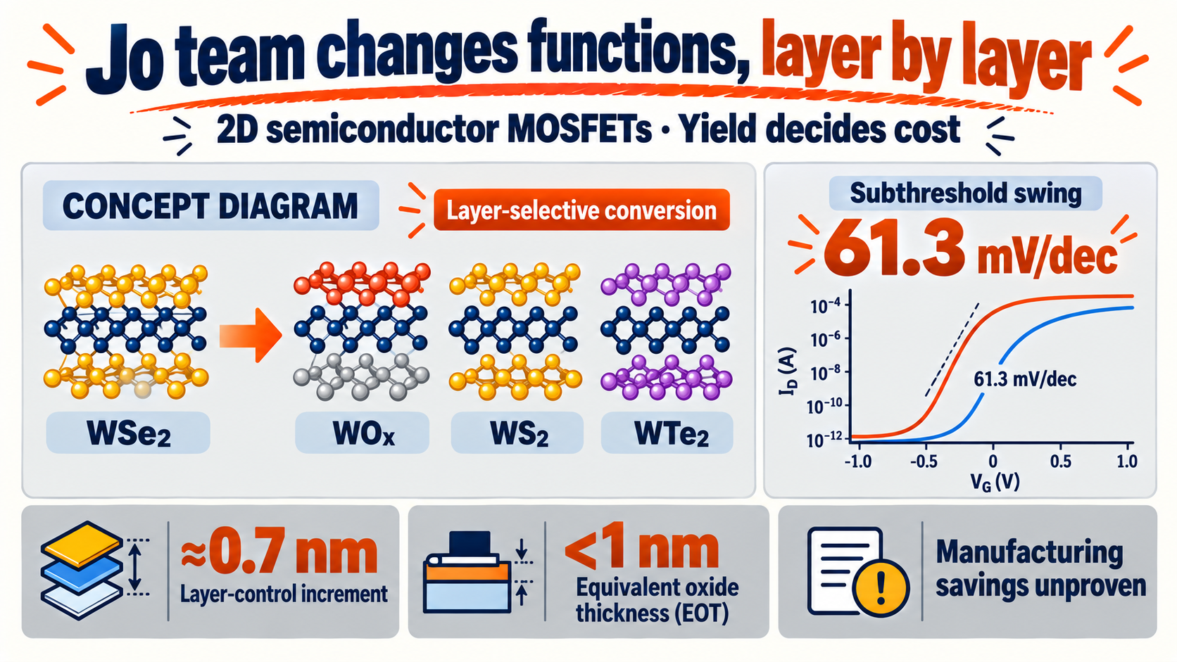
Moon-Ho Jo, director of the IBS Center for Van der Waals Quantum Solids and a distinguished professor at POSTECH, leads a new approach to 2D semiconductor MOSFETs. His team changes selected layers in roughly 0.7nm increments. The industrial question is whether that control can ultimately make chips cheaper. Source: 과기정통부·정책브리핑
The Science publication date is October 15, 2026; the Korean announcement specifies 3 a.m. on October 16. This is a device study, not a measurement of manufacturing savings. Device results and factory economics need separate treatment. Source: 과기정통부·게재 시각
Moon-Ho Jo, Seok Young Min and Hyunje Cho
Seok Young Min and Hyunje Cho share the leading-author marker in the IBS publication list, which identifies Jo as corresponding author. Suk-Ho Lee and Jaeho Choi are among their collaborators. Public institutional materials do not establish individual measurement assignments. Source: IBS 논문 목록
Jo’s work connects atomic-scale materials growth with electronic devices. His recent publications include ultrascaled MoS₂ transistors in 2024 and single-crystalline monolayer growth in 2025. The new study extends that line of work toward integrating materials with different electronic roles. Source: IBS 조문호 프로필
2D semiconductor MOSFETs need more than thin channels
A MOSFET is a voltage-controlled switch. It needs a channel carrying current, a gate controlling that channel, and insulation separating them. It also needs effective electrical contacts. A narrow pipe is little use if its connections obstruct the flow.
Atomically thin channels are attractive, but their relatively unreactive surfaces complicate uniform dielectric deposition. Jo’s team addresses this integration problem. Reducing the burden of joining the semiconductor, insulation and contacts could help translate channel properties into useful devices. Source: imec 2D 소자 로드맵
Existing processes already use many materials and carefully engineered interfaces. The novelty is not the first use of multiple materials. It is creating different functions by converting selected parts of an existing parent material.
What Min and Cho changed, layer by layer
Min and Cho start from tungsten diselenide, WSe₂. Selected regions become insulating WOₓ, n-type WS₂ or semimetallic WTe₂; unconverted WSe₂ remains available as a channel. Sulfur, selenium and tellurium belong to the chalcogen family. Source: 과기정통부·물질 전환
Conversion involves chemical processing, including oxidation and subsequent vapor reactions. Temperature, pressure and interlayer gaps help control depth; masks define lateral regions. The roughly 0.7nm increment describes layer control, not a technology-node name or gate length. Source: 과기정통부·층과 위치 제어
Channel
WSe₂ semiconductor
Retained material
Insulation
WOₓ dielectric
Converted material
Contacts and n-type option
WTe₂ semimetal
Contact layer
n-type · WS₂ semiconductor
In n-type devices, electrons are the main carriers; in p-type devices, holes play that role. Digital circuits use both. A bandgap is the energy separation between occupied states and states that can carry conduction current. The method offers a way to create distinct electronic functions from a shared starting material.
What 61.3mV does—and does not—tell us
Jo’s devices reported a subthreshold swing of 61.3mV per decade: the gate-voltage change associated with a tenfold current change. That approaches the conventional room-temperature MOSFET limit of about 60mV/dec; it does not break it. Source: 과기정통부·스위칭 측정
About 60 is the conventional room-temperature reference; 61.3 is reported. Not a speed or chip-power comparison. · Axis starts at 59, not zero
Equivalent oxide thickness, or EOT, was below 1nm. EOT expresses electrical gate coupling as an equivalent silicon-dioxide thickness; it is neither the physical film thickness nor the whole transistor size. An on/off current ratio above ten million describes current separation, not computing speed. Source: 과기정통부·EOT와 전류비
The reported injection barrier fell to 35.5meV, about a third of the direct-metal-contact comparison. That is an energy barrier, not a proportional reduction in resistance, power or cost. Circuit-level benefits still depend on drive current, wiring and leakage. Source: 과기정통부·접합 장벽
A vertically stacked complementary inverter demonstrates signal inversion. The IBS English release also describes a separate MoS₂ nFET using WOₓ insulation. It would therefore be misleading to claim that every part of the complete circuit came exclusively from one WSe₂ crystal. An inverter is an initial circuit demonstration, not processor qualification. Source: IBS 제공 영문 설명
Manufacturing economics depend on usable output
The following is economic analysis, not a reported cost result. If Min and Cho’s approach removes some transfer or interface operations, it could reduce tool visits and queue time. More wafers per tool could improve productivity. Extra conversion, masking, cleaning and inspection time could offset those gains.
What matters is total manufacturing cost divided by usable output. Consider a hypothetical equal-die-count example: baseline total cost 100 and yield 90%. If a new process costs 90 but yields only 75%, its cost per good die is 108 relative to the baseline. A 10% reduction in process spending can coexist with an 8% increase per usable chip.
Baseline=100. Normalize total cost/yield; equal die count and performance assumed. Not IBS measurements or forecasts. · Axis starts at 81, not zero
These are assumed values, not IBS yields or savings forecasts. Performance, die count and test scope are held constant to isolate yield. If conversion reaches too many or too few layers, inspection and resulting losses must be included. A wafer-wide distribution matters more than a single excellent device.
Where the 300mm race leaves Korean equipment and materials suppliers
The manufacturing benchmark facing Jo’s work is advancing. In June 2026, imec, ASML and TSMC reported a separate 300mm 2D-device process with a 50nm contacted poly pitch. CPP accounts for contact space as well as the gate: a short channel alone does not ensure a dense chip. Source: imec·ASML·TSMC, 2026-06-15
The collaboration reported 94% operational transistors under an Imax/Imin >10⁵ criterion. That is not a 94% finished-chip yield and is not a result from the Science conversion process. The comparison highlights the distance between a materials method and repeatable manufacturing. Source: imec·작동 소자 판정 기준
For Korean suppliers, the opportunity may lie in equipment controlling reaction depth, high-purity process materials and rapid defect metrology. These are possible demand channels, not forecasts of orders for named firms. A research process must also satisfy customers’ contamination and maintenance requirements.
Adoption could begin with devices complementing silicon logic. Imec describes learning through less demanding planar 2D devices. Under that scenario, Jo’s method would be a candidate for selected modules. This could limit initial capital requirements, while leaving substantial integration and qualification work. Source: imec·단계적 도입 전략
If circuits eventually deliver adequate performance at lower voltage, battery-powered sensing and local computation could gain new options. New markets require energy or battery savings large enough to offset early chip premiums. Difficult integration could instead confine the approach to specialized devices. Neither outcome follows automatically from this paper.
Manufacturers must still address wiring and contact losses after changing a channel. Our earlier CoSi interconnect article provides a related view of why a materials improvement needs several further validations before it changes whole-chip economics. Our 7eV oxide semiconductor article looks at the insulating side of the same problem. Related: 관련 글: CoSi 반도체 배선
What Jo’s team still has to prove
This 2D semiconductor MOSFET study expands the options for creating and connecting electronic functions. Next come large-area conversion uniformity, lasting insulation and contact performance, and the cost of equivalent circuits. Industrial competitiveness requires matched power, speed and lifetime conditions.
Jo, Min and Cho offer a new processing option at atomic-layer scale. The question for industry is whether that option can work within a practical manufacturing line and lower cost per saleable chip. The next stage is to answer with comparable production data.
Source scope: the Science full text and supplements were inaccessible. Research figures were checked against the official ministry account and IBS release; authorship and research history against IBS pages. Sample counts, long-term reliability and production costs were not established by those materials. Economic scenarios are illustrative analysis, not investment advice.
Evaluate layer conversion by the cost of a usable chip at matched performance.
Sources and further reading
- Science — Modular van der Waals MOSFETs through layer-by-layer chalcogen substitutions
- 과학기술정보통신부·정책브리핑 — 원자층 골라 바꿔 반도체 만든다 (2026-10-16)
- IBS — 연구단 논문 목록
- IBS — Director Moon-Ho Jo
- IBS 제공 영문 발표 — Turning single 2D crystal into a complete high-performance transistor (2026-10-15)
- imec — Introducing 2D-material based devices in the logic scaling roadmap
- imec·ASML·TSMC — 300mm 2D transistor integration (2026-06-15)
For information only — this is not a recommendation to buy or sell any asset.
Comments 0